Your cart is currently empty!
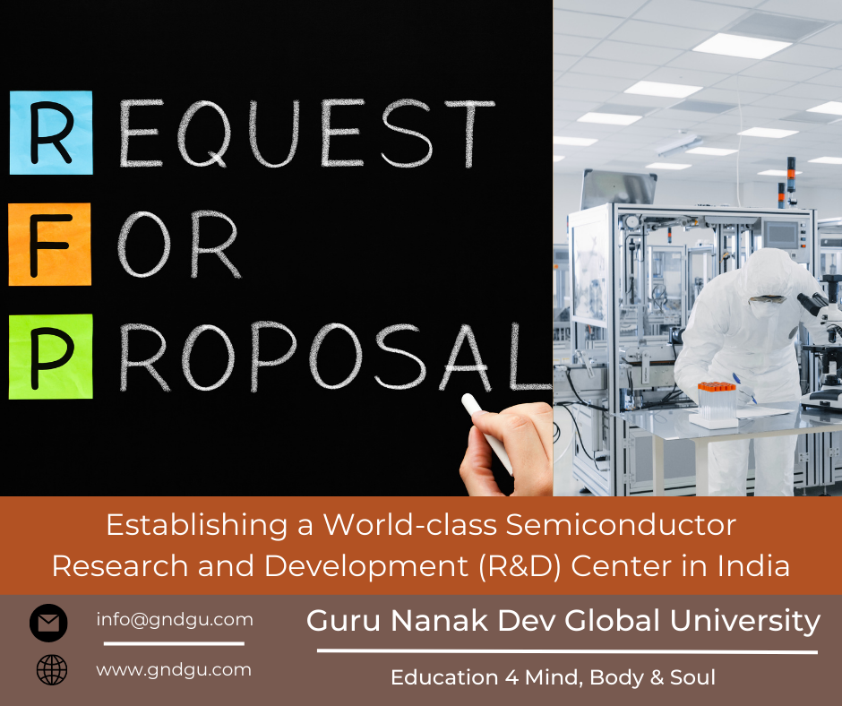
Request for Proposal (RFP): Establishing a World-class Semiconductor Research and Development (R&D) Center in India
1. Introduction:
Guru Nanak Dev Global University, hereinafter referred to as “GNDGU,” is seeking proposals from qualified organizations and entities interested in collaborating to establish a state-of-the-art semiconductor Research and Development (R&D) Center in India. The R&D center aims to drive innovation, enhance technological capabilities, and contribute to the growth of the semiconductor industry. This Request for Proposal (RFP) outlines the scope of work, submission guidelines, evaluation criteria, and other relevant details.
2. Brief: Setting up a 200mm Wafer Size Semiconductor R&D Center in India
Overview:
The establishment of a 200mm wafer size semiconductor research and development (R&D) center in India with a strong focus on developing innovative processes and conducting research on materials is a strategic initiative aimed at enhancing technological capabilities, driving innovation and beyond , and positioning India as a global player in the semiconductor industry. This brief outlines the key considerations and priorities for setting up such a center, including facility requirements, research focus, talent acquisition, and partnerships.
Facility Requirements:
The R&D center will be equipped with state-of-the-art facilities, including cleanrooms with stringent environmental controls, specialized laboratories for materials research and process development, and advanced equipment suitable for 28nm semiconductor fabrication. Adequate space for equipment installation, storage, and future expansion should be considered. The facility should also have infrastructure support for utilities, waste management, and safety measures in compliance with industry standards.
Research Focus:
The R&D center’s primary objective should be to develop innovative processes and conduct research on materials for the 28nm and beyond semiconductor technology. This includes exploring new fabrication techniques, optimizing existing processes, and evaluating novel materials to improve device performance and reliability. The center should foster a collaborative environment that encourages interdisciplinary research, knowledge sharing, and cross-functional expertise to drive technological advancements.
Talent:
GNDGU would be recruiting or partnering with organizations with highly skilled and experienced workforce which is crucial for the success of the R&D center. Partnering with organizing or hiring researchers, engineers, and scientists with expertise in semiconductor physics, materials science, process engineering, and device design is essential. The center would also focus on talent development by offering training programs, internships, and collaboration opportunities with academia and research institutions to nurture a skilled workforce in the field of semiconductor research and development.
Partnerships and Collaborations:
Establishing partnerships and collaborations with industry leaders, academic institutions, and research organizations is vital for the R&D center’s success. Collaborative projects, joint research initiatives, and technology transfer programs with these entities can accelerate innovation, facilitate knowledge sharing, and access additional resources. Partnering with equipment suppliers and material manufacturers can also provide access to cutting-edge technologies and resources for research and development activities.
Setting up a 200mm wafer size semiconductor R&D center in India with a focus on innovative processes and research on materials requires careful planning, state-of-the-art facilities, a talented workforce, and strategic partnerships. By prioritizing these aspects, the R&D center can drive advancements in semiconductor technology, contribute to the growth of the industry, and position India as a global hub for semiconductor research and development.
3. India Semiconductor Policy
The India Semiconductor Policy, implemented by the Government of India, is a strategic framework aimed at promoting and developing the semiconductor industry within the country. The policy’s primary objectives are to enhance India’s competitiveness in the global semiconductor market, attract investments, foster innovation, and create employment opportunities in the semiconductor sector. By implementing this policy, the government aims to position India as a major player in the semiconductor industry.
In line with the policy’s objectives, the Ministry of Electronics and IT recently announced the reopening of applications for the Semicon India Program. Both old and new applicants are invited to submit their proposals, subject to meeting the government’s criteria. It has been noted that the government expressed dissatisfaction with the applications for the more expensive 28nm fabs. To ensure a rigorous evaluation process, the investment proposals will be assessed by the India Semiconductor Mission, a specialized body responsible for overseeing the semiconductor sector’s development.
To encourage investment and facilitate the establishment of semiconductor facilities, the application window for the “Modified Scheme for Setting up of Compound Semiconductors / Silicon Photonics/Sensors Fab/Discrete Semiconductors Fab and Semiconductor ATMP/OSAT facilities in India” will remain open until December 2024. This scheme aims to attract various semiconductor-related projects and technologies to the country, aligning with the overarching goals of the India Semiconductor Policy. By extending the application window, the government aims to provide ample opportunity for interested parties to participate in the development of India’s semiconductor industry.
GNDGU is looking for potential partners for establishing a world-class Semiconductor Research Center in India under this program.
4. Scope of Work:
The GNDGU Semiconductor R&D Center in India will focus on the following areas:
- Conducting cutting-edge research in semiconductor technology and applications.
- A research center with a strong focus on processes and materials for the 28nm and beyond.
- Developing and testing advanced semiconductor components and devices.
- Enhancing the competitiveness of India in the global semiconductor industry.
- Providing a platform for collaboration between industry, academia, and research institutions.
- Creating employment opportunities and fostering skill development in the semiconductor field.
- Proposal Submission Guidelines:
5. Proposal Deadline:
Monday, August 21st, 2023 by 5:00p.m EST
6. Contact for Inquiries:
For any inquiries or clarifications regarding this RFP, please contact
Baljit Singh
Founding Member, Guru Nanak Dev Global University
Phone: +1-972-800-6305
Email: info@gndgu.com
7. Proposal Format:
Please submit your proposal in PDF format, with a maximum 30 pages. The proposal should be organized into sections according to the outlined structure.
i. Organization Overview:
Provide a concise overview of your educational institute or organization, including its history, mission, and areas of expertise related to semiconductor research and development.
ii. Experience:
Highlight any previous experience in establishing and operating R&D centers or similar facilities, especially in the semiconductor industry.
iii. Technical Expertise and Capabilities:
Demonstrate your organization’s technical expertise in the semiconductor field, particularly in areas such as semiconductor materials, device fabrication, process optimization, system integration, and advanced research.
iv. Resources:
Outline the capabilities and resources you can bring to the proposed R&D center, including infrastructure, equipment, and access to research facilities.
v. Collaborative Approach:
Describe your organization’s approach to collaboration and knowledge sharing with industry, academia, and research institutions. Highlight any successful collaborations or partnerships that demonstrate your ability to foster innovation and drive advancements in semiconductor technology.
vi. Project Plan and Timeline:
Present a detailed plan outlining the key milestones, activities, and timeline for supporting us for establishing and/or operating the R&D center in India. Specify the phased approach, resource allocation, and any potential risks or challenges.
vii. Human Resources:
Describe the personnel and expertise with their brief profile to support and successfully implement the project plan.
viii. Financial Considerations:
Provide a comprehensive financial plan if any, including investment requirements, funding sources, and anticipated revenue streams.
ix. Collaboration and Support from Government and Academic Institutions:
Describe any existing collaborations or partnerships with government entities and academic institutions in the field of semiconductor.
8. Evaluation Criteria:
- Technical Expertise: Demonstrated expertise and experience in semiconductor research and development.
- Collaborative Approach: The proposed approach to collaboration and knowledge sharing with industry, academia, and research institutions.
- Project Plan: The feasibility and effectiveness of the project plan, including milestones, timeline, and resource allocation.
- Financial Viability: The financial plan and projections, including investment requirements and expected return on investment.
- Experience and Track Record: Past experience and success in establishing and operating Semiconductor R&D centers or similar facilities.
- Alignment with Objectives: The extent to which the proposal aligns with the objectives of the R&D center.
- Proposal Submission:
9. Submission Details
Please submit your proposal electronically to info@gndgu.com no later than 5:00p.m EST, Monday, August 21st, 2023 by 5:00p.m EST.
The subject line of the email should be “Proposal Submission – Establishing R&D Center – [Your Organization Name].”
We look forward to receiving your proposal and exploring the opportunity to collaborate in establishing a world-class semiconductor R&D center in India.
About Guru Nanak Dev Global University
Guru Nanak Dev Global University is committed to being a global leader in education, research, and positive social impact. Our vision is to create a transformative educational institution that empowers students with the knowledge, skills, and global perspective needed to excel in a rapidly evolving world. We strive to establish a vibrant and inclusive campus that serves as a hub for cultural exchange, academic excellence, research, innovation, and community engagement.
Mission Statement
“TO PROVIDE A WORLD-CLASS EDUCATION AND PROMOTE EXCELLENCE IN RESEARCH, INNOVATION, AND HOLISTIC DEVELOPMENT, WITH A STRONG FOCUS ON PRACTICAL KNOWLEDGE, WHILE NURTURING THE VALUES OF COMPASSION, EQUALITY, AND SOCIAL RESPONSIBILITY BASED ON GURU NANAK DEV’S TEACHINGS. OUR AIM IS TO POSITION GURU NANAK DEV GLOBAL UNIVERSITY AMONG THE TOP 200 ACADEMIC UNIVERSITIES IN GLOBAL RANKINGS, UPHOLDING THE PRINCIPLES OF GURU NANAK DEV AND PREPARING STUDENTS TO BECOME ENLIGHTENED GLOBAL CITIZENS WHO ACTIVELY CONTRIBUTE TO SOCIETY.”
Guru Nanak Dev Global University takes immense pride in being the world’s first university with its Mission Goals aligned to the UNESCO’s 17 Sustainable Development Goals (SDGs). We recognize the critical importance of addressing global challenges and promoting sustainable development for the betterment of society and the planet.
By aligning our Mission Goals with the SDGs, we are committed to actively contributing to the achievement of these goals. Our university’s vision, educational programs, research initiatives, and community engagement efforts are designed to align with the principles and targets set forth by UNESCO for sustainable development.
Through our comprehensive approach to education, research, and social impact, we aim to make a positive and tangible difference in areas such as poverty eradication, quality education, gender equality, clean water and sanitation, sustainable energy, economic growth, reduced inequalities, sustainable cities and communities, responsible consumption and production, climate action, biodiversity conservation, and more.
By integrating the SDGs into our curriculum, fostering interdisciplinary research, and promoting sustainable practices on campus, we empower our students to become agents of change who actively contribute to addressing these global challenges. We believe that education is a powerful tool for creating a sustainable future, and we strive to equip our students with the knowledge, skills, and values necessary to make a meaningful impact in their respective fields and communities.
At Guru Nanak Dev Global University, we place a strong emphasis on promoting cross-cultural understanding and embracing diversity. Our aim is to foster an environment that celebrates and respects individuals from all backgrounds. Through high-quality education, we endeavor to cultivate leaders who are not only academically competent but also globally aware, socially responsible, and culturally sensitive.
We are committed to pushing the boundaries of knowledge and addressing pressing societal challenges. Through innovative teaching methods, interdisciplinary research, and collaboration with renowned scholars and industry experts, we aim to contribute to the advancement of various fields, including religion, history, herbal sciences, music, politics, and more.
Community engagement and sustainable development are at the core of our university’s mission. We actively participate in the social, cultural, and economic growth of the region, striving to be a catalyst for positive change. By encouraging students and faculty to engage in community service, outreach programs, and partnerships with local organizations, we aim to make a lasting impact.
We aspire to foster global citizenship among our students, equipping them with the skills, intercultural competencies, and international experiences necessary to thrive in an interconnected world. We believe in the power of mutual respect, dialogue, and collaboration to create responsible global citizens and leaders who contribute to positive change on a global scale.
Join us at Guru Nanak Dev Global University, where knowledge knows no boundaries, and the pursuit of excellence is fueled by a passion for global understanding and shared experiences. Be a part of a university that is actively working towards creating a better world for current and future generations. Together, we can make a significant contribution to the attainment of the SDGs and build a more sustainable and inclusive society.
One response to “Request for Proposal (RFP): Establishing a World-class Semiconductor Research and Development (R&D) Center in India”
Very nice afford 👌 congratulations I am with you ❤️