Learn the Language of Semiconductors
NEXUS–SEMICON | THE SEMICONDUCTOR CAREER CODE
From Getting a Job to Building a Career
A semiconductor career does not begin with a job title.
It begins with understanding.
Whether you want to become a process engineer, equipment engineer, design engineer, product engineer, yield engineer, packaging engineer, technician, researcher, project manager, or technology leader – you need to understand the fundamental language of the semiconductor industry.
You don’t have to become an expert in every area.
But you should know how the pieces fit together.
This is the focus of Week 4 of The Semiconductor Career Code: Build Your Technical Foundation.
Why Technical Fundamentals Matter
The semiconductor industry is one of the most interconnected industries in the world.
A decision made during material selection can influence device performance.
A change in process parameters can affect yield.
A transistor design can influence power consumption.
A manufacturing defect can affect reliability.
Packaging can influence thermal performance.
And a small improvement at one stage of the manufacturing process can have a significant impact on the final cost and performance of a semiconductor device.
This is why semiconductor professionals need more than isolated technical knowledge.
They need systems thinking.
You should be able to look at the semiconductor value chain and understand:
Material → Device → Circuit → Wafer → Process → Chip → Package → System
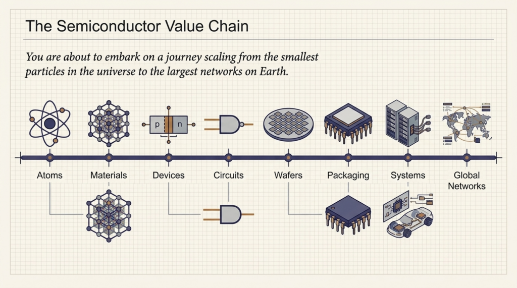
That understanding begins with the fundamentals.
1. Start With Atoms and Electrons
Everything begins with matter.
At the heart of semiconductor technology is our understanding of atoms, electrons, and how electrons behave.
Electrons carry electrical charge.
Their movement – and our ability to control that movement – is fundamental to semiconductor technology.
When we learn about semiconductor devices, we are essentially learning how to control the behavior of charge carriers to perform useful functions.
That simple idea eventually leads us to computers, smartphones, artificial intelligence accelerators, automobiles, communication systems, medical devices, and countless other technologies.
2. Conductors, Insulators and Semiconductors
Before understanding a semiconductor, understand what makes it different.
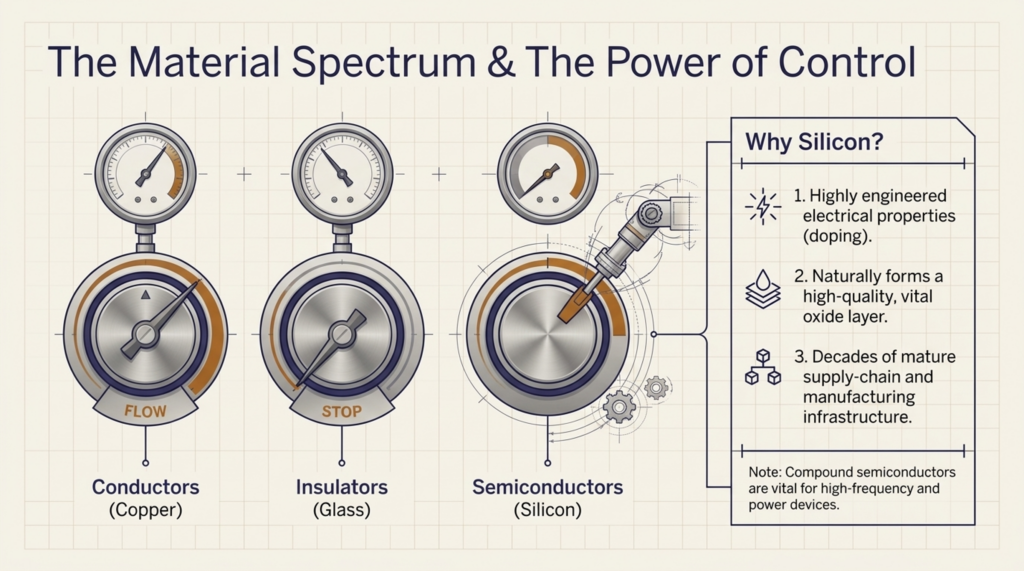
Conductors
Conductors allow electric charge to move relatively easily.
Examples include metals such as copper and aluminum.
Insulators
Insulators strongly resist the movement of electric charge.
Examples include glass, rubber, and many forms of ceramic and polymer materials.
Semiconductors
Semiconductors occupy the fascinating middle ground.
Their electrical behavior can be controlled.
And that controllability is what makes them so valuable.
A semiconductor isn’t simply “halfway between” a conductor and an insulator.
Its real power comes from our ability to engineer its electrical properties.
That is the foundation of modern electronics.
3. Why Silicon?
When people talk about semiconductors, they frequently talk about silicon.
Why?
Silicon has several characteristics that make it extremely useful for semiconductor manufacturing.
It has suitable electrical properties, can be engineered through doping, and forms a high-quality oxide layer that is extremely important in many semiconductor devices and manufacturing processes.
Silicon also benefits from decades of manufacturing infrastructure, process knowledge, equipment development, and supply-chain maturity.
But remember:
Semiconductors are not synonymous with silicon.
Other semiconductor materials, including compound semiconductors; play important roles in applications such as high-frequency electronics, optoelectronics, and power devices.
4. Doping: Engineering the Semiconductor
Pure semiconductor material is not enough for most practical devices.
We modify its electrical properties through a process called doping.
Doping introduces controlled impurities into a semiconductor crystal.
This allows engineers to create regions with different electrical characteristics.
Two fundamental concepts are:
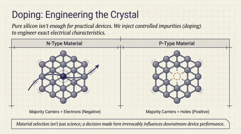
N-type material
Associated with electrons as the majority carriers.
P-type material
Associated with holes as the majority carriers.
Doping is one of the fundamental techniques that allows engineers to transform semiconductor material into functional electronic devices.
5. The PN Junction
Bring P-type and N-type semiconductor regions together and you create a PN junction.
This simple structure is one of the foundational concepts in semiconductor electronics.
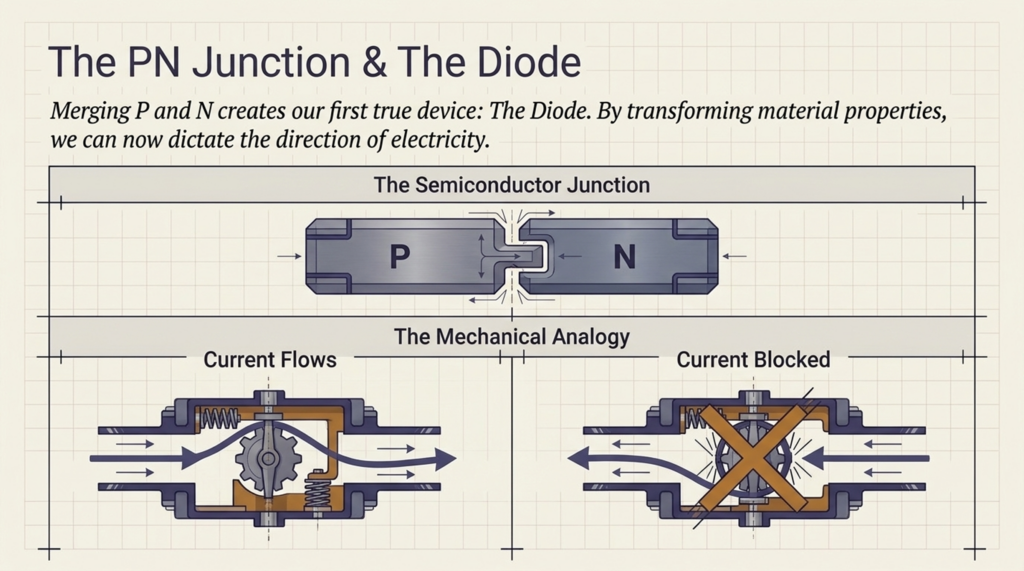
The behavior of the PN junction gives us the basis for understanding devices such as diodes and, more broadly, many semiconductor structures.
Understanding the PN junction is therefore an important milestone in your technical journey.
6. The Diode
A diode is one of the simplest semiconductor devices.
At a conceptual level, it provides a way to control the direction in which current can flow under appropriate conditions.
Diodes are used in:
- Rectification
- Protection
- Signal processing
- Voltage regulation
- Switching
- Power electronics
- Light-emitting devices
If you understand the PN junction, you are already beginning to understand how semiconductor devices transform material properties into useful electrical functions.
7. The Transistor: The Building Block of Modern Computing
Now we reach one of the most important concepts in semiconductor technology:
The transistor.
A transistor is a semiconductor device that can control electrical current and is fundamental to switching and amplification.
Modern digital electronics rely heavily on transistors acting as switches.
Think about that for a moment.
Your smartphone.
Your laptop.
A data center.
An AI accelerator.
An automobile’s electronic control systems.
All depend on enormous numbers of semiconductor devices.
At the heart of modern digital computing is the ability to control electrical behavior at extremely small scales.
The Week 4 challenge:
Explain a transistor to a non-engineer in three minutes.
If you can explain it clearly without hiding behind technical terminology, you are demonstrating something more important than memorization.
You are demonstrating understanding.
8. CMOS: The Foundation of Modern Digital Logic
CMOS- Complementary Metal-Oxide-Semiconductor; is one of the most important technologies in modern digital electronics.
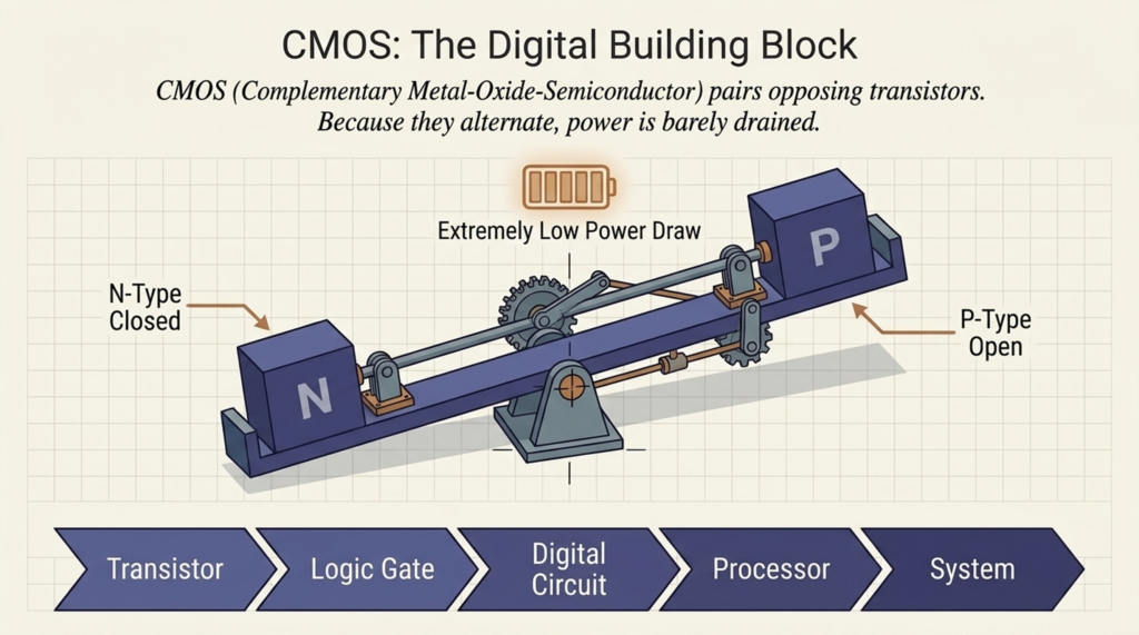
CMOS logic uses complementary transistor structures to implement digital circuits efficiently.
It became foundational to modern integrated circuit design because of its favorable power characteristics and scalability.
From logic gates to processors, memory, controllers, and complex system-on-chip devices, CMOS technology has played a central role in the evolution of modern electronics.
Understanding CMOS helps you connect:
Transistor → Logic Gate → Digital Circuit → Processor → System
9. Integrated Circuits: From Individual Devices to Systems
Imagine building a computer using individual discrete transistors.
It would be enormous, expensive, difficult to manufacture, and extremely unreliable.
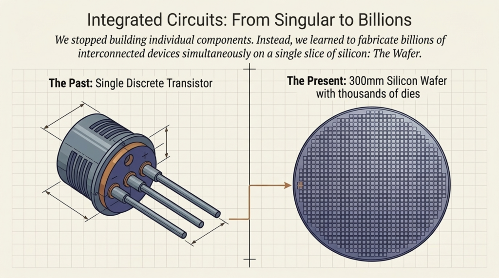
Integrated circuits changed the game.
Instead of treating every electronic component as a separate device, engineers learned how to fabricate enormous numbers of devices and interconnections on semiconductor substrates.
The result?
Integrated circuits.
Modern chips can contain billions of transistors.
That level of integration is one of the defining achievements of modern engineering.
10. The Wafer: Where the Chip Begins
A semiconductor chip doesn’t start as a chip.
It begins on a wafer.
A wafer is a thin slice of semiconductor material, commonly silicon, on which semiconductor devices are fabricated.
During manufacturing, many individual integrated circuits—or dies—are created across the wafer.
A simplified manufacturing journey looks something like:
Wafer → Deposition → Patterning → Etching → Doping → Cleaning → Inspection → Metallization → Testing → Dicing → Packaging
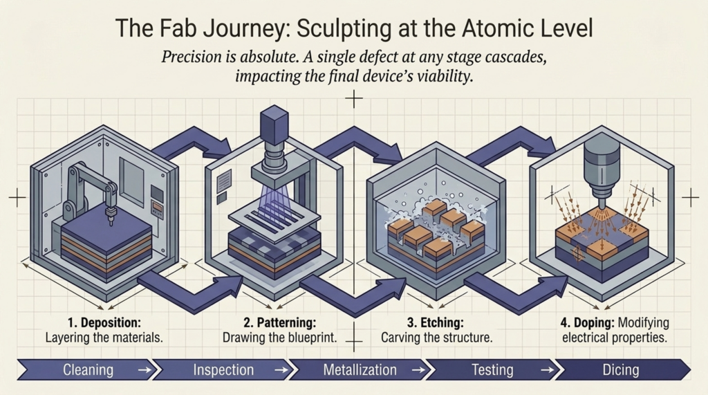
Each stage requires extraordinary precision.
And each stage can influence final device performance and yield.
11. Process Nodes: More Than Just a Number
You will frequently hear terms such as:
7 nm
5 nm
3 nm
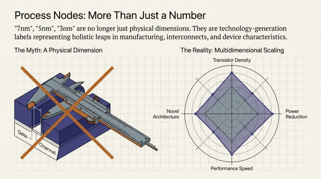
These are commonly referred to as process nodes.
But here’s an important career lesson:
Don’t assume that a process-node number simply represents one physical dimension of every feature on a modern chip.
Today, process-node names are better understood as technology-generation labels associated with a broader set of manufacturing and device characteristics.
As technology advances, engineers work on:
- Smaller and more efficient devices
- Greater transistor density
- Improved performance
- Reduced power consumption
- New transistor architectures
- Advanced interconnects
- More sophisticated manufacturing processes
Understanding the evolution of process technology helps you understand why semiconductor engineering is so challenging.
12. Yield: The Business of Manufacturing
A semiconductor device can work perfectly in a laboratory and still fail as a commercial product.
Why?
Because manufacturing millions of devices is a completely different challenge.
Yield is a critical semiconductor manufacturing metric.
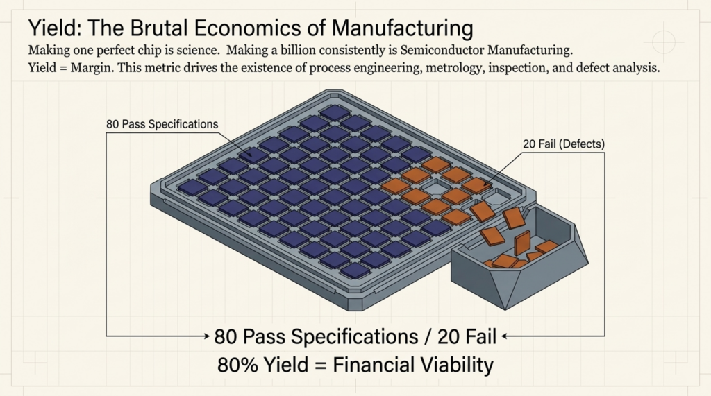
At a high level, it represents the proportion of manufactured devices meeting the required specifications.
Imagine producing 1,000 chips.
If only 800 meet the required specifications, your yield is approximately 80%.
Improving yield can have enormous economic value.
This is why semiconductor manufacturing is not only about making devices work.
It is about making them work consistently, reliably, and economically at scale.
That is where process engineering, equipment engineering, metrology, inspection, statistical analysis, defect engineering, and yield engineering become critically important.
13. Packaging: The Chip Needs a Home
A semiconductor die is not the final product.
It must be packaged and connected to the outside world.
Packaging provides electrical connections, mechanical protection, thermal management, and increasingly sophisticated integration capabilities.
Modern packaging has become a major area of innovation.
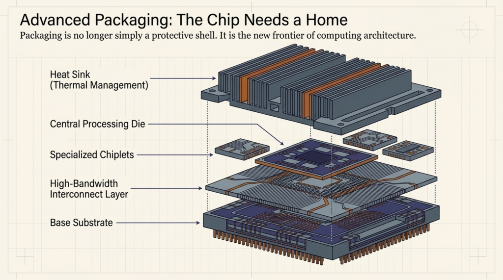
Advanced packaging approaches can enable:
- Heterogeneous integration
- Chiplets
- High-bandwidth interconnects
- Improved thermal management
- Greater system-level performance
- Integration of different technologies
This means packaging is no longer simply the final step after fabrication.
It is increasingly part of the architecture of advanced computing systems.
The Big Picture
Now connect everything.
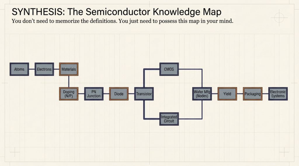
Start with:
Atoms
↓
Electrons
↓
Semiconductor Materials
↓
Doping
↓
PN Junction
↓
Diodes & Transistors
↓
CMOS
↓
Integrated Circuits
↓
Wafer Manufacturing
↓
Process Technology
↓
Yield
↓
Packaging
↓
Electronic Systems
This is your Semiconductor Fundamentals Knowledge Map.
The goal isn’t to memorize this sequence.
The goal is to understand the relationships.
The Three-Minute Transistor Challenge
This week’s activity is intentionally simple:
Explain a transistor to someone who knows nothing about electronics.
You have three minutes.
Don’t start with equations.
Don’t start with semiconductor physics.
Don’t overwhelm them with terminology.
Try explaining the fundamental idea:
A transistor is a device that allows us to control electrical behavior.
In digital electronics, transistors can function as extremely fast electronic switches.
By combining enormous numbers of these switches, engineers can build logic circuits.
Those circuits can perform calculations.
Those calculations enable processors, memory systems, AI accelerators, communication systems, and countless other technologies.
If you can communicate that idea clearly, you are beginning to move from knowing terminology to understanding technology.
Your Week 4 Deliverable
Create your own:
SEMICONDUCTOR FUNDAMENTALS KNOWLEDGE MAP
Your map should connect at least these concepts:
Atoms → Electrons → Conductors/Insulators/Semiconductors → Silicon → Doping → P-Type/N-Type → PN Junction → Diode → Transistor → CMOS → Integrated Circuit → Wafer → Process Node → Yield → Packaging
Then add one more layer:
“Why does this matter?”
For every concept, write one sentence explaining its role in the semiconductor ecosystem.
This simple exercise can reveal where your technical foundation is strong—and where you need to learn more.
A Career Lesson From Week 4
One of the biggest mistakes early-career professionals make is trying to learn semiconductor technology by memorizing hundreds of isolated terms.
Don’t.
Build connections.
When you hear yield, think about manufacturing.
When you hear doping, think about controlling semiconductor properties.
When you hear CMOS, think about transistor-level digital logic.
When you hear wafer, think about fabrication.
When you hear packaging, think beyond protection—think system integration.
When you hear process node, think about technology generation and scaling.
The objective isn’t to know every answer.
The objective is to know where the answer fits.
From Getting a Job to Building a Career
A strong semiconductor career is built in layers.
Layer 1 – Fundamentals
Understand the technology.
Layer 2 – Technical Depth
Develop expertise in a specific domain.
Layer 3 – Problem Solving
Learn to diagnose and solve real problems.
Layer 4 – Systems Thinking
Understand how your work affects other functions.
Layer 5 – Communication
Next week we jump into Communication – Explain complex ideas clearly.
The Semiconductor Career Code
The semiconductor industry is creating opportunities across engineering, manufacturing, design, equipment, materials, software, data, packaging, supply chain, operations, quality, and leadership.
You don’t need to know everything.
But you do need to be curious.
You need to ask:
How does it work?
Why does it work?
What can make it fail?
How do we improve it?
How does my work affect the next stage?
Those questions are the beginning of engineering thinking.
And engineering thinking is the foundation of a semiconductor career.
NEXUS–SEMICON
THE SEMICONDUCTOR CAREER CODE
52 Weeks. 52 Skills. One Career Journey.
From Getting a Job → Building a Career.
#NEXUSSemicon #SemiconductorCareerCode #Semiconductors #SemiconductorIndustry #Microelectronics #Silicon #Transistors #CMOS #IntegratedCircuits #Wafer #SemiconductorManufacturing #YieldEngineering #Packaging #EngineeringCareers #STEMCareers #FutureOfSemiconductors #CareerDevelopment #TechnicalSkills #EngineeringLeadership