NEXUS–SEMICON | THE SEMICONDUCTOR CAREER CODE
Theme: Become Known for Something
In the semiconductor industry, technical capability gets you into the conversation, but professional visibility, credibility, and a clear identity help people remember you.
Week 5 is about building a professional brand that answers three questions:
Who are you?
What do you know?
Why should someone remember you?
Your goal is not to create a flashy personal brand. Your goal is to build a credible professional identity around your semiconductor knowledge, experience, skills, achievements, interests, and future direction.
1. WEEK 5 LEARNING OBJECTIVES
By the end of Week 5, participants should be able to:
- Define their professional identity.
- Identify their semiconductor specialization or area of interest.
- Build a strong LinkedIn profile.
- Create a semiconductor-focused resume.
- Develop a professional portfolio.
- Write a compelling professional biography.
- Establish a technical profile.
- Begin developing thought leadership.
- Audit their digital footprint.
- Create a consistent professional message across platforms.
Week 5 Core Principle
Your professional brand is the intersection of:
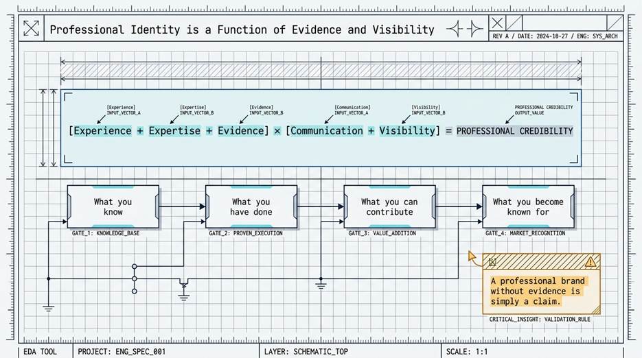
Experience + Expertise + Evidence + Communication + Visibility
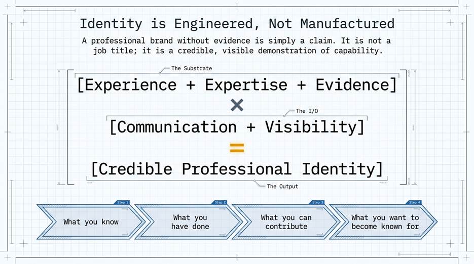
A professional brand without evidence is simply a claim.
A strong semiconductor professional brand shows:
What you know → What you have done → What you can contribute → What you want to become known for.
2. WHAT IS A PROFESSIONAL BRAND?
Your professional brand is the perception people develop about your:
- Expertise
- Skills
- Experience
- Character
- Communication
- Technical interests
- Professional contribution
- Industry knowledge
- Career direction
It is not merely your job title.
For example:
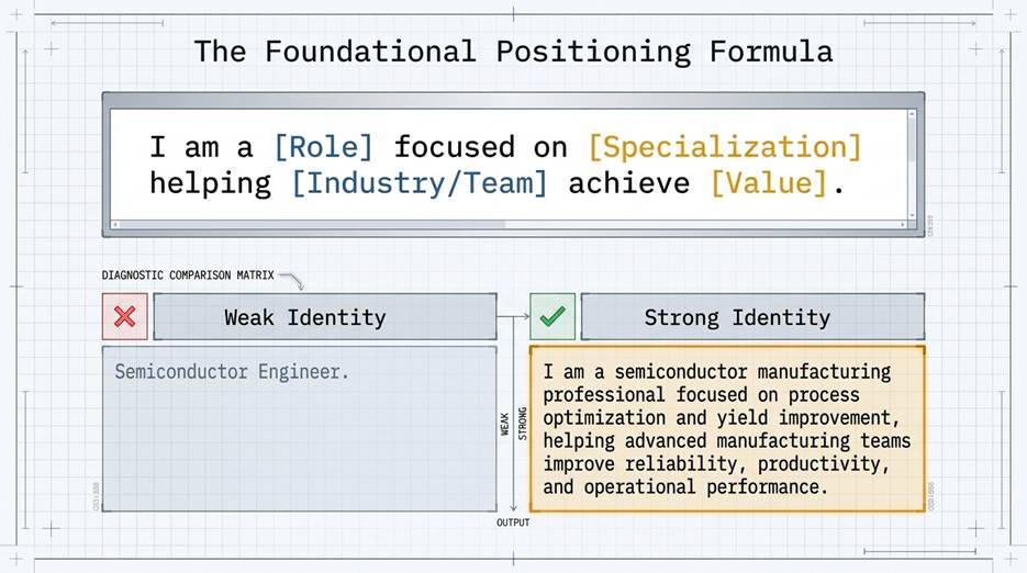
Weak identity:
Semiconductor Engineer
Stronger identity:
Semiconductor process engineer focused on advanced manufacturing, yield improvement, process integration, and semiconductor equipment technologies.
The second statement tells people what the person cares about and contributes to.
3. THE SEMICONDUCTOR PROFESSIONAL BRAND MODEL
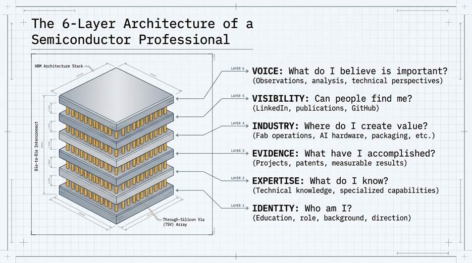
Use this framework:
IDENTITY: Who am I?
Your education, experience, role, background and professional direction.
EXPERTISE: What do I know?
Your technical knowledge and specialized capabilities.
EVIDENCE: What have I accomplished?
Projects, publications, patents, designs, improvements, certifications, research and measurable results.
INDUSTRY: Where do I create value?
Fab operations, semiconductor equipment, materials, design, packaging, testing, AI hardware, power semiconductors, sensors, manufacturing, etc.
VISIBILITY: Can people find and understand me?
LinkedIn, publications, presentations, portfolio, GitHub, professional organizations and industry participation.
VOICE: What do I believe is important in my field?
Your observations, analysis, lessons learned and technical perspectives.
4. TOPIC 1 – PERSONAL BRAND
A personal brand begins with positioning.
Ask: Who are you professionally?
Examples:
- Semiconductor process engineer
- IC design engineer
- Equipment engineer
- Yield engineer
- Packaging engineer
- Semiconductor manufacturing professional
- Materials scientist
- Device physicist
- Semiconductor sales professional
- Technical project manager
- Semiconductor supply-chain professional
- Semiconductor business-development professional
- Semiconductor researcher
- Emerging semiconductor professional
Then identify your specialization.
Formula
I am a [role] focused on [specialization] helping [industry/company/team] achieve [value].
Example:
I am a semiconductor manufacturing professional focused on process optimization and yield improvement, helping advanced manufacturing teams improve reliability, productivity and operational performance.
5. FIND YOUR “KNOWN FOR”
The theme of Week 5 is:
Become Known for Something.
You don’t need to be known for everything.
You need to become associated with a specific area of value.
Possible semiconductor brand territories:
Technology
- Semiconductor process technology
- Advanced nodes
- CMOS
- Power semiconductors
- MEMS
- Compound semiconductors
- Silicon carbide
- Gallium nitride
- Photonics
- Semiconductor packaging
Engineering
- Process integration
- Yield engineering
- Equipment engineering
- Reliability
- Device engineering
- Test engineering
- Design verification
- Manufacturing engineering
Business
- Semiconductor strategy
- Supply chain
- Business development
- Market intelligence
- Technical sales
- Investment
- Partnerships
- Manufacturing strategy
Emerging Areas
- AI semiconductors
- Chiplets
- Advanced packaging
- HBM
- Edge computing
- Automotive semiconductors
- Semiconductor sustainability
- Semiconductor workforce development
6. TOPIC 2 – LINKEDIN
Your LinkedIn profile should function as your professional landing page.
When someone searches your name, they should quickly understand:
Who you are + what you do + what you know + what you have accomplished.
LinkedIn Profile Architecture
1. Professional photo
Use:
- Clear head-and-shoulders image
- Professional appearance
- Simple background
- Good lighting
- Current photograph
2. Headline
Avoid simply:
Engineer at XYZ Company
Instead communicate expertise.
Formula:
Role | Semiconductor Expertise | Technical Specialty | Industry Focus
Example:
Semiconductor Engineer | Process Integration | Yield & Manufacturing | Advanced Semiconductor Technologies
7. LINKEDIN ABOUT SECTION
Your About section should answer:
Who are you?
What do you specialize in?
What have you accomplished?
What problems do you enjoy solving?
What are you interested in?
What opportunities or conversations are you open to?
Suggested structure
Paragraph 1 – Identity
Who you are professionally.
Paragraph 2 – Expertise
Your technical and business capabilities.
Paragraph 3 – Evidence
Major accomplishments, projects, research or results.
Paragraph 4 – Industry interests
What areas of semiconductors you follow.
Paragraph 5 – Future direction
What you want to contribute next.
8. LINKEDIN EXPERIENCE
Don’t simply list responsibilities.
Convert responsibilities into impact statements.
Weak
Responsible for process monitoring.
Stronger
Monitored semiconductor manufacturing processes and analyzed process data to identify opportunities for yield and process stability improvements.
Even stronger
Analyzed process performance data to identify variation drivers and supported improvement initiatives focused on yield, process stability and manufacturing efficiency.
Whenever possible include:
Action + Technology + Problem + Result
9. LINKEDIN FEATURED SECTION
Use the Featured section as your professional showcase.
Potential content:
- Technical articles
- Publications
- Research
- Presentations
- Conference presentations
- Projects
- Patents
- Portfolio
- Technical videos
- Industry analysis
- Awards
- Certifications
Think of it as:
“Show me what you can do.”
10. TOPIC 3 – RESUME
A semiconductor resume should communicate technical capability and measurable contribution.
Recommended structure
Name
Professional Title
Professional Summary
Technical Skills
Professional Experience
Major Projects
Education
Certifications
Publications / Patents
Professional Organizations
Awards / Recognition
11. SEMICONDUCTOR RESUME FORMULA
Use:
Action + Technology + Problem + Result
For example:
Developed process-monitoring methodology for semiconductor manufacturing operations, improving visibility into process variation and supporting yield-improvement initiatives.
Instead of:
Worked on process monitoring.
12. QUANTIFY YOUR ACHIEVEMENTS
Numbers create credibility.
Where appropriate, include:
- Yield improvement
- Cost reduction
- Cycle-time reduction
- Equipment uptime
- Defect reduction
- Productivity improvement
- Revenue supported
- Number of projects
- Number of customers
- Team size
- Process improvements
- Patents
- Publications
- Products launched
For example:
Reduced process cycle time by X%.
Supported X manufacturing tools across multiple production areas.
Led a cross-functional team of X engineers.
Supported deployment of X semiconductor manufacturing systems.
Don’t invent numbers.
If an achievement cannot be quantified, explain its scope and impact.
13. TOPIC 4 – PORTFOLIO
Your resume tells people what you have done.
Your portfolio shows them.
A semiconductor professional portfolio might include:
Engineering
- Design projects
- Simulation work
- Process analysis
- Device modeling
- Test projects
- Manufacturing projects
Research
- Papers
- Research summaries
- Experimental results
- Technical presentations
Business
- Market analysis
- Semiconductor industry reports
- Competitive analysis
- Market-entry research
Leadership
- Projects led
- Teams managed
- Programs launched
- Industry initiatives
14. THE “3-PROJECT PORTFOLIO”
If you don’t have a portfolio, start with three projects.
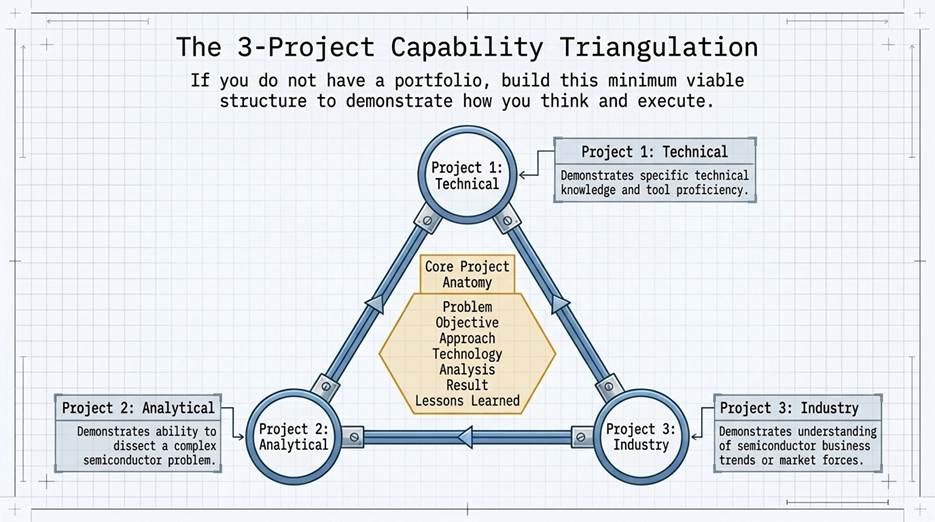
Project 1 – Technical
Demonstrate technical knowledge.
Project 2 – Analytical
Demonstrate your ability to analyze a semiconductor problem.
Project 3 – Industry
Demonstrate your understanding of semiconductor business or industry trends.
Each project should include:
Problem
Objective
Approach
Technology
Analysis
Result
Lessons Learned
15. TOPIC 5 – TECHNICAL PROFILE
A technical profile should make your capabilities easy to understand.
Create a technical skills matrix.
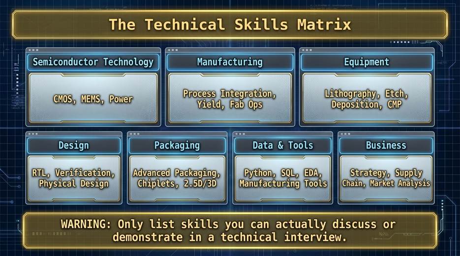
Only list skills you can actually discuss or demonstrate.
16. TOPIC 6 – PROFESSIONAL BIOGRAPHY
Your professional biography is different from your resume.
A resume says:
Here is my professional history.
A biography says:
Here is my professional story.
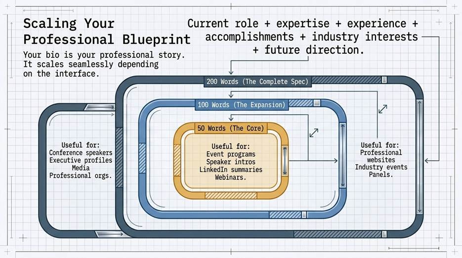
50-word bio
Useful for:
- Event programs
- Speaker introductions
- Webinars
- Conferences
100-word bio
Useful for:
- Professional websites
- Industry events
- Publications
- Panels
200-word bio
Useful for:
- Conference speakers
- Executive profiles
- Professional organizations
- Media profiles
17. PROFESSIONAL BIO FORMULA
Use:
Current role + expertise + experience + accomplishments + industry interests + future contribution
Example:
[Name] is a semiconductor professional specializing in [area]. With experience in [areas], [Name] has worked on [projects/technologies]. Their interests include [topics], with a particular focus on [specialization]. They are passionate about advancing [industry contribution].
Keep it factual.
Don’t fill your biography with exaggerated adjectives.
18. TOPIC 7 – THOUGHT LEADERSHIP
Thought leadership does not mean pretending to know everything.
It means consistently sharing useful knowledge and informed perspectives.
Start small.
Content ideas
Write about:
- What you learned this week
- A semiconductor technology you studied
- An industry trend
- A technical concept explained simply
- A manufacturing challenge
- A semiconductor supply-chain issue
- A research paper you found interesting
- A conference lesson
- A career lesson
- A project lesson
19. THE 5–5–5 CONTENT MODEL
Create:
5 technical posts
Explain semiconductor concepts.
5 industry posts
Discuss industry developments and trends.
5 professional posts
Share lessons from your career and projects.
This creates a foundation of 15 pieces of professional content.
20. THE “TEACH ONE THING” RULE
Every post should ideally teach the reader something.
Instead of:
Semiconductor technology is fascinating.
Write:
One reason advanced semiconductor manufacturing becomes increasingly difficult at smaller geometries is the growing sensitivity to process variation. Here’s what that means for yield…
The second creates a reason for someone to read.
21. TOPIC 8 – DIGITAL FOOTPRINT
Your digital footprint is everything people can discover about you online.
Audit:
- Personal website
- Publications
- GitHub
- Google search results
- Professional organizations
- Conference profiles
- Social media
- Old portfolios
- Public comments
- Public presentations
Ask:
If a semiconductor hiring manager searched my name today, what would they learn about me?
22. DIGITAL FOOTPRINT AUDIT
Search your name.
Look at the first several results.
Create three categories:
KEEP
Professional and relevant.
IMPROVE
Useful but incomplete or outdated.
REMOVE / RESTRICT
Content that is inappropriate, misleading, outdated or unnecessarily public.
The objective isn’t to create a fake online identity.
It is to make sure your professional identity is accurate and consistent.
23. BRAND CONSISTENCY
Your:
- Resume
- Portfolio
- Biography
- Email signature
- Conference profile
should tell the same professional story.
For example, if your LinkedIn says:
Semiconductor Manufacturing & Yield
but your resume says:
Software Developer
and your portfolio focuses on:
Semiconductor Packaging
people may struggle to understand your direction.
Your materials don’t need identical wording, but they should have a coherent professional narrative.
24. CREATE YOUR SEMICONDUCTOR BRAND STATEMENT
Complete this:
I am a __________ specializing in __________.
My expertise includes __________, __________ and __________.
I am particularly interested in __________.
I create value by __________.
I want to become known for __________.
This becomes the foundation for your:
- LinkedIn headline
- About section
- Resume summary
- Professional bio
- Portfolio
- Networking introduction
25. 30-SECOND PROFESSIONAL INTRODUCTION
Participants should be able to introduce themselves clearly.
Formula
Name + Role + Expertise + Industry Interest + Value
Example:
“I’m Alex. I’m a semiconductor process engineer focused on manufacturing and yield improvement. My background is in process analysis and equipment optimization, and I’m particularly interested in advanced semiconductor manufacturing and next-generation process technologies.”
Simple.
Specific.
Memorable.
26. WEEK 5 ACTIVITY
BUILD YOUR SEMICONDUCTOR PROFESSIONAL PROFILE
Participants will spend the week building their professional identity.
STEP 1 – Identify your niche
Choose:
- Primary expertise
- Secondary expertise
- Industry interest
- Future specialization
STEP 2 – Create your brand statement
Write your:
“I am…” statement.
STEP 3 – Rewrite your LinkedIn profile
Update:
- Photo
- Headline
- About
- Experience
- Skills
- Featured section
- Education
- Certifications
STEP 4 = Rewrite your resume
Create a semiconductor-focused resume.
STEP 5 – Create your professional bio
Write:
- 50-word bio
- 100-word bio
- 200-word bio
STEP 6 – Build your portfolio
Identify at least three projects or accomplishments.
STEP 7 – Audit your digital footprint
Search your name and evaluate what appears.
STEP 8 – Publish
Create your first professional LinkedIn post related to your semiconductor expertise.
27. WEEK 5 DELIVERABLE
THE SEMICONDUCTOR PROFESSIONAL BRAND PACKAGE
Every participant completes:
1. Resume
One professional semiconductor-focused resume
2. LinkedIn
Fully optimized LinkedIn profile
3. Professional Biography
50–100 word professional biography
Recommended additions:
- Professional headline
- Technical skills matrix
- Portfolio
- Professional introduction
- First thought-leadership post
- Digital footprint audit
28. WEEK 5 SELF-ASSESSMENT
Rate yourself from 1–5 on each area:
| Area | Score |
| I can clearly explain my professional identity | ___/5 |
| My LinkedIn communicates my expertise | ___/5 |
| My resume demonstrates measurable value | ___/5 |
| I have a clear technical profile | ___/5 |
| I have a professional biography | ___/5 |
| I have evidence of my capabilities | ___/5 |
| I have a portfolio | ___/5 |
| I can explain what I want to be known for | ___/5 |
| I regularly share professional knowledge | ___/5 |
| My digital footprint supports my career | ___/5 |
The purpose isn’t the number.
The purpose is identifying where your professional brand needs work.
29. WEEK 5 KEY LESSONS
Lesson 1
Your title is not your brand.
Lesson 2
Your expertise needs evidence.
Lesson 3
Your resume tells your history; your portfolio demonstrates capability.
Lesson 4
LinkedIn is not simply an online resume—it is part of your professional presence.
Lesson 5
Thought leadership begins by teaching what you know.
Lesson 6
Consistency creates credibility.
Lesson 7
You don’t need to become famous. You need to become useful and recognizable within your professional area.
30. WEEK 5 CHALLENGE
THE “KNOWN FOR ONE THING” CHALLENGE
Choose one semiconductor topic you want people to associate with you.
For the next 30 days:
Learn about it.
Write about it.
Talk about it.
Build something around it.
Connect with people working in it.
Share what you learn.
Your objective:
Become increasingly recognizable for a specific area of semiconductor knowledge.
31. WEEK 5 FINAL MESSAGE
Your professional brand isn’t something you manufacture overnight.
It is built through consistent evidence of who you are and what you can contribute.
Your resume tells people where you’ve been.
Your LinkedIn tells people who you are professionally today.
Your portfolio shows what you can do.
Your biography tells your story.
Your thought leadership demonstrates how you think.
Your digital footprint tells the world what you have chosen to make visible.
And together, they answer one important question:
“What do you want to be known for?”
WEEK 5 → BUILD YOUR PROFESSIONAL BRAND
Don’t just look for your next opportunity.
Build a professional identity that makes your capabilities visible when the opportunity arrives.