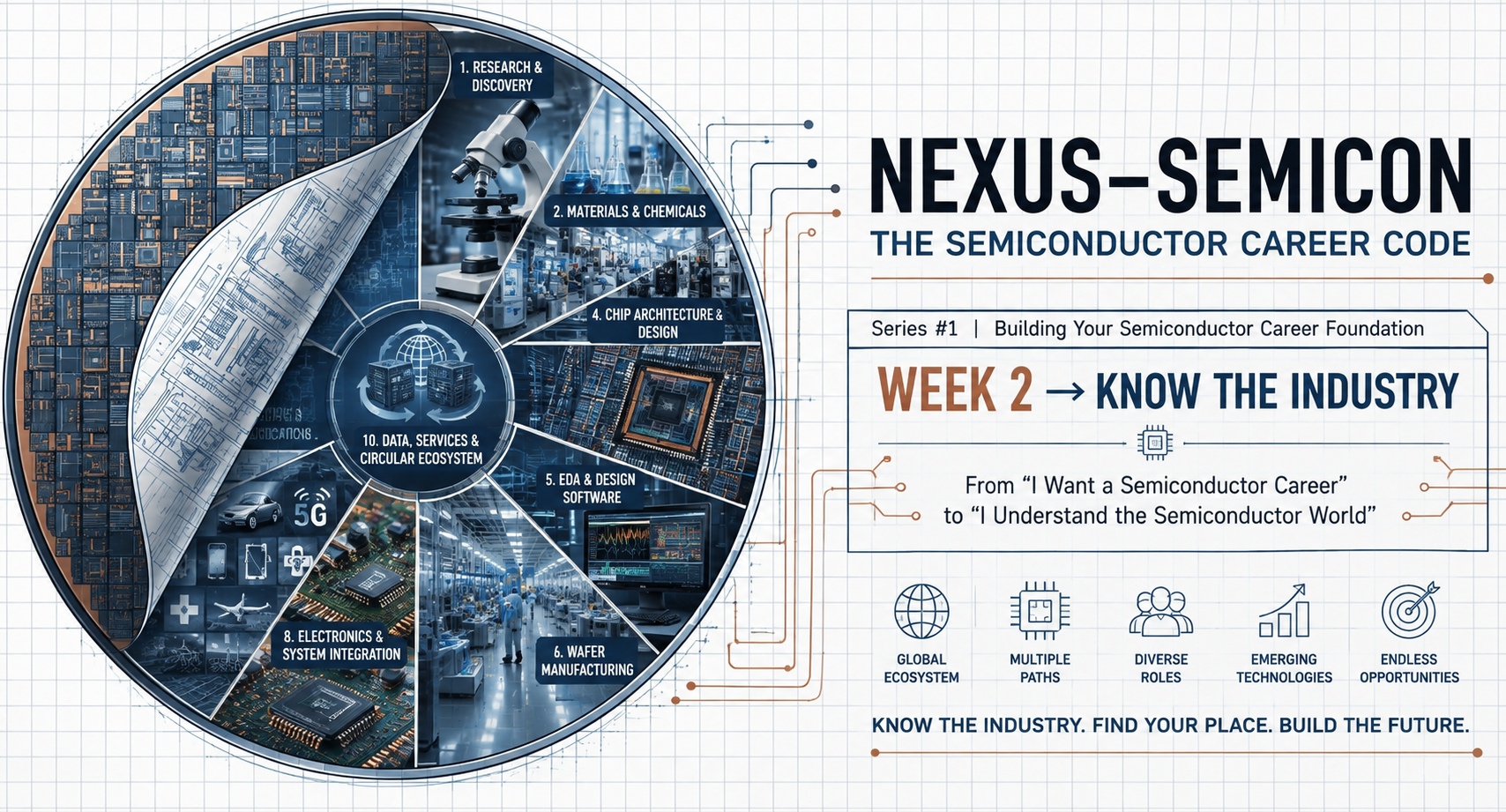
NEXUS–SEMICON
Semiconductor Technology & Systems
Series #2 / 52 | KNOW THE INDUSTRY
From “I Want a Semiconductor Career” to “I Understand the Semiconductor World”
Welcome to Week 2
Last week, we began with the most important person in your career: you.
Week 1 | Know Yourself – was about understanding your interests, strengths, curiosity, capabilities, values, and aspirations.
But self-awareness alone does not build a career.
A successful semiconductor professional must understand the industry they want to enter.
That is the purpose of Week 2.
Welcome to:
WEEK 2 | KNOW THE INDUSTRY
The semiconductor industry is much larger than the word “chip” suggests.
It is an interconnected global ecosystem involving materials, equipment, design, software, intellectual property, manufacturing, packaging, testing, electronics, systems, data, artificial intelligence, energy, transportation, communications, defense, healthcare and countless other applications.
If you understand only one part of this ecosystem, you see a piece of the picture.
If you understand how the pieces connect, you begin to see where opportunities are created; and where your career can create value.
1. Why You Must Know the Industry
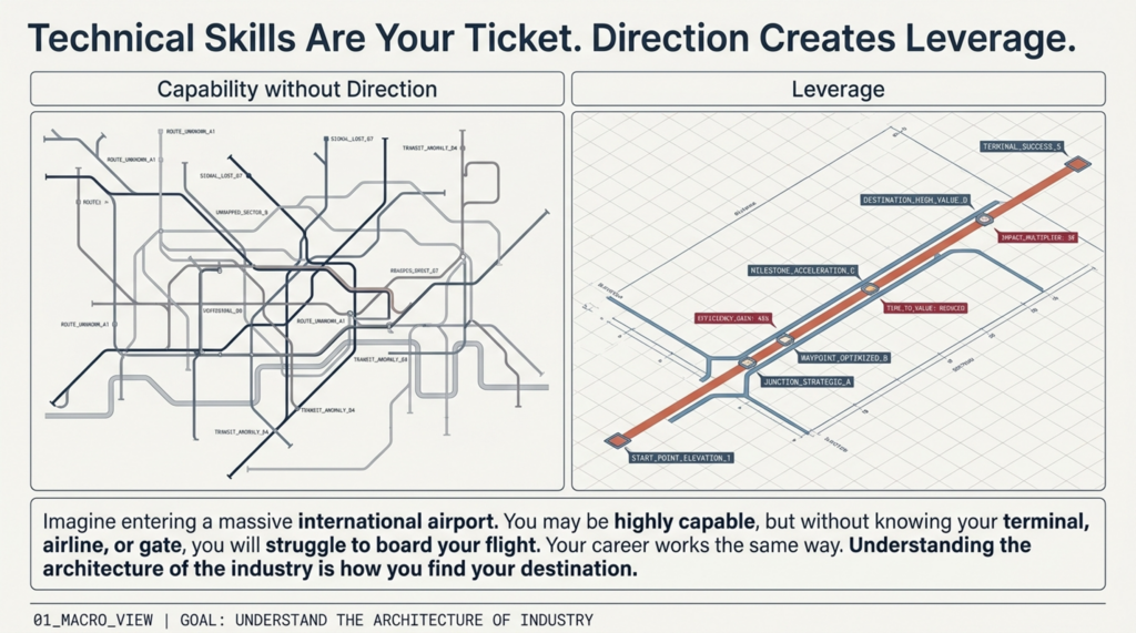
Imagine entering an airport without knowing:
- where you are going,
- which terminal you need,
- which airline you are flying,
- what gate you need,
- or when boarding begins.
You may be highly capable—but you will still struggle to reach your destination.
Your career works the same way.
Technical skills are important.
But direction creates leverage.
Understanding the semiconductor industry helps you answer:
- What are the major sectors of industry?
- Who are the major players?
- How does a semiconductor move from an idea to a finished product?
- What technologies are driving growth?
- Where are the biggest talent shortages?
- Which skills are becoming more valuable?
- Which parts of the value chain are growing?
- Where are new manufacturing opportunities emerging?
- What roles exist beyond traditional engineering?
- How can I position myself before entering the workforce?
The goal is not to memorize companies.
The goal is to understand the architecture of industry.
2. The Semiconductor Industry Is an Ecosystem
A semiconductor does not simply begin in a factory and end in a computer.
The journey is much longer.
A simplified semiconductor value chain looks like this:
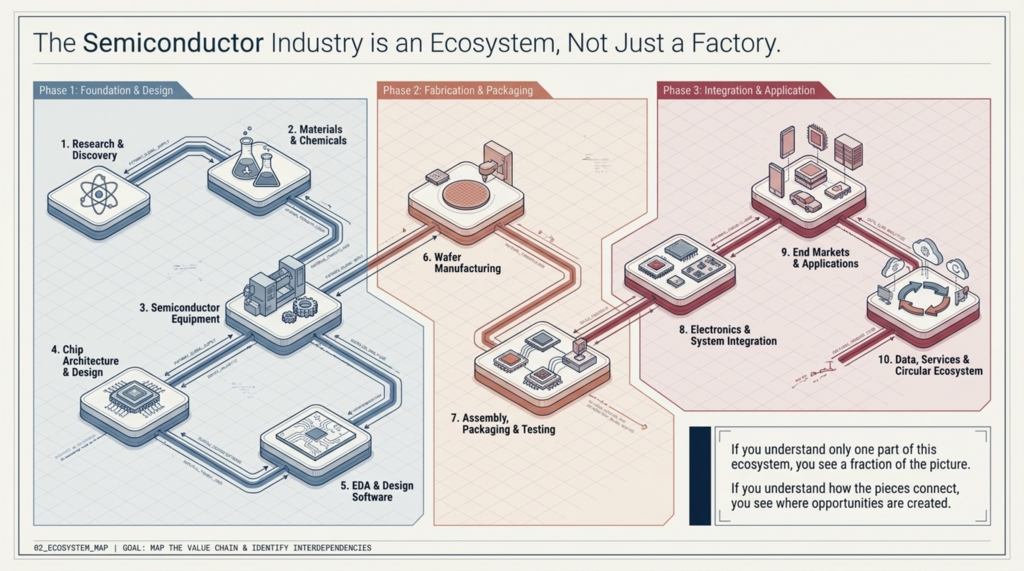
Research & Discovery -> Materials & Chemicals -> Semiconductor Equipment -> Chip Architecture & Design -> EDA & Design Software -> Wafer Manufacturing -> Assembly, Packaging & Testing -> Electronics & System Integration -> End Markets & Applications -> Data, Services & Circular Ecosystem
Each stage creates careers.
Each stage requires different skills.
And each stage depends on the others.
3. Learn the Semiconductor Value Chain
A. Semiconductor Materials
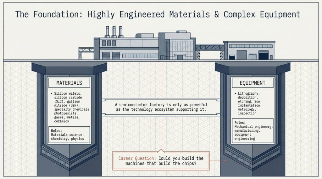
Before a chip can be manufactured, manufacturers need highly engineered materials.
Examples include:
- silicon wafers,
- silicon carbide,
- gallium nitride,
- specialty chemicals,
- photoresists,
- gases,
- metals,
- ceramics,
- quartz,
- CMP materials,
- packaging materials,
- substrates.
This creates opportunities in:
- materials science,
- chemistry,
- physics,
- process engineering,
- quality,
- supply chain,
- manufacturing,
- equipment engineering.
Career Question
Could you become the person who develops, qualifies, manufactures or manages the materials that make semiconductor manufacturing possible?
4. Semiconductor Equipment
Semiconductor manufacturing requires extraordinarily sophisticated equipment.
Equipment categories include:
- lithography,
- deposition,
- etching,
- ion implantation,
- cleaning,
- oxidation,
- diffusion,
- CMP,
- metrology,
- inspection,
- wafer handling,
- packaging,
- testing.
The equipment industry is itself a major technology ecosystem.
This means a semiconductor career does not require you to work for a chip manufacturer.
You can build a career designing, manufacturing, installing, maintaining or improving the machines that manufacture chips.
Key Insight
A semiconductor factory is only as powerful as the technology ecosystem supporting it.
5. Chip Design
At the other end of the manufacturing spectrum is semiconductor design.
Design engineers determine:
- what the chip does,
- how it processes information,
- how much power it consumes,
- how fast it operates,
- how much area it occupies,
- how it communicates with other systems.
Important areas include:
- digital design,
- analog design,
- mixed-signal design,
- RF,
- memory,
- power management,
- processors,
- GPUs,
- AI accelerators,
- automotive chips,
- connectivity,
- security.
Design increasingly connects with:
- artificial intelligence,
- machine learning,
- software,
- architecture,
- verification,
- cybersecurity.
6. EDA: The Software Behind Chip Design
Modern chips are too complex to design manually.
Engineers rely on sophisticated Electronic Design Automation (EDA) tools.
EDA supports activities such as:
- simulation,
- verification,
- physical design,
- synthesis,
- timing analysis,
- layout,
- modeling,
- design-for-manufacturing.
This creates a powerful intersection between:
Semiconductors + Software + Mathematics + AI
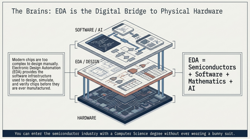
A computer science student can therefore enter the semiconductor industry without becoming a traditional semiconductor process engineer.
7. Wafer Fabrication
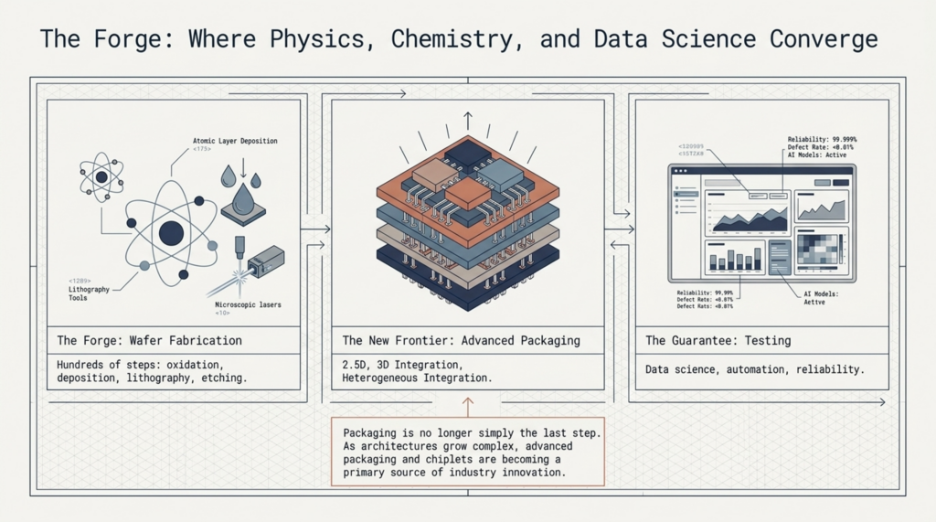
The wafer fabrication facility or fab is where semiconductor devices are physically created on wafers.
The process involves hundreds of tightly controlled steps.
These can include:
- wafer preparation,
- oxidation,
- deposition,
- lithography,
- etching,
- implantation,
- annealing,
- cleaning,
- metallization,
- inspection,
- metrology.
The environment demands:
- precision,
- process control,
- contamination control,
- automation,
- statistical analysis,
- reliability,
- quality systems.
This is where physics, chemistry, electrical engineering, mechanical engineering, chemical engineering and data science converge.
8. Packaging and Testing
A semiconductor is not finished when the wafer leaves fabrication.
Individual dies must be:
- separated,
- assembled,
- packaged,
- connected,
- tested,
- qualified.
Modern packaging has become a major technology frontier.
Important areas include:
- advanced packaging,
- 2.5D packaging,
- 3D integration,
- chiplets,
- heterogeneous integration,
- high-bandwidth memory integration,
- thermal management,
- advanced substrates.
As semiconductor architectures become increasingly complex, packaging is no longer simply the “last step.”
It is becoming a major source of innovation.
9. Semiconductor Testing
Every semiconductor product must demonstrate that it works reliably.
Testing can occur at multiple stages:
- wafer test,
- die test,
- package test,
- system-level test,
- reliability testing.
Testing requires:
- automated test equipment,
- instrumentation,
- software,
- data analysis,
- failure analysis,
- reliability engineering.
This creates career opportunities for electrical engineers, computer engineers, software engineers, data scientists, technicians and automation specialists.
10. Semiconductor Applications
The semiconductor industry ultimately exists because chips enable products and systems.
Semiconductors power:
Artificial Intelligence
AI accelerators, GPUs, CPUs, memory and networking.
Automotive
ADAS, electric vehicles, power electronics, sensors and autonomous systems.
Telecommunications
5G, future wireless networks, RF devices and optical communications.
Consumer Electronics
Smartphones, computers, wearables and smart appliances.
Industrial Automation
Robotics, sensors, motor control and factory automation.
Aerospace & Defense
High-reliability processors, sensors, communications and power systems.
Healthcare
Imaging, diagnostics, wearable devices and medical instrumentation.
Energy
Solar, energy storage, power conversion and smart grids.
Quantum Technologies
Specialized devices, control electronics and emerging quantum architectures.
Internet of Things
Sensors, connectivity, edge computing and ultra-low-power devices.
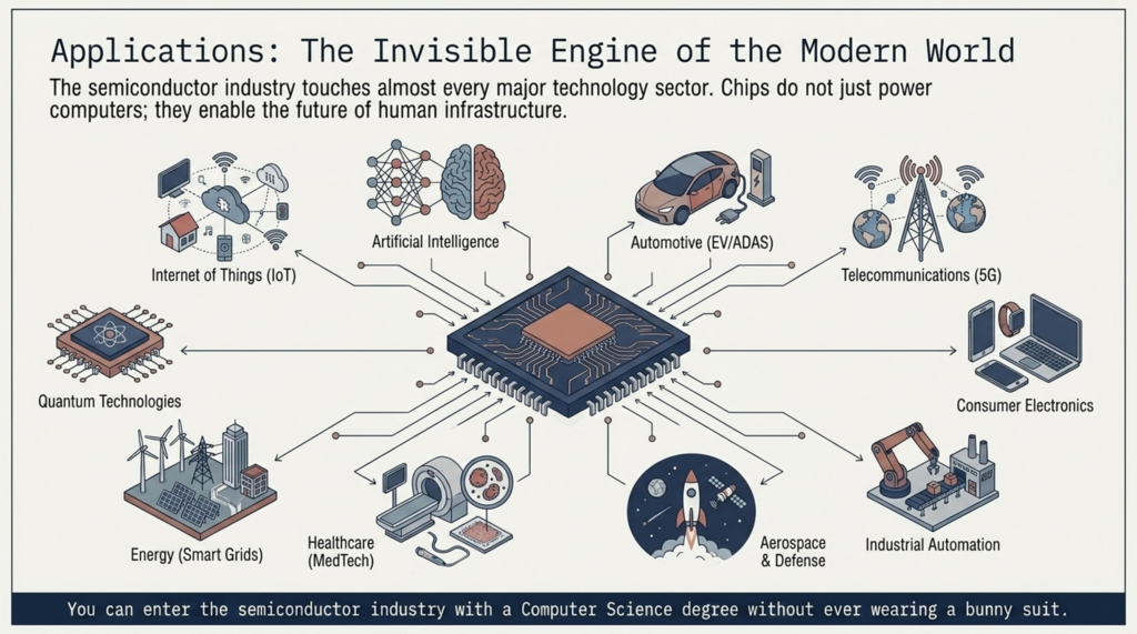
The semiconductor industry therefore touches almost every major technology sector.
11. Understand the Different Semiconductor Business Models
One of the most important things to understand is that semiconductor companies do not all operate the same way.
IDMs — Integrated Device Manufacturers
These companies may design and manufacture their own semiconductor products.
Fabless Companies
These companies primarily design chips while outsourcing manufacturing.
Foundries
Foundries manufacture semiconductor devices for other companies.
OSAT Companies
Outsourced Semiconductor Assembly and Test companies specialize in packaging and testing.
Equipment Companies
These companies build the machines used to manufacture semiconductors.
Materials Companies
They supply wafers, chemicals, gases, substrates and other critical inputs.
EDA Companies
They provide the software infrastructure used to design and verify chips.
IP Companies
They develop reusable semiconductor intellectual property such as processor cores and interface technologies.
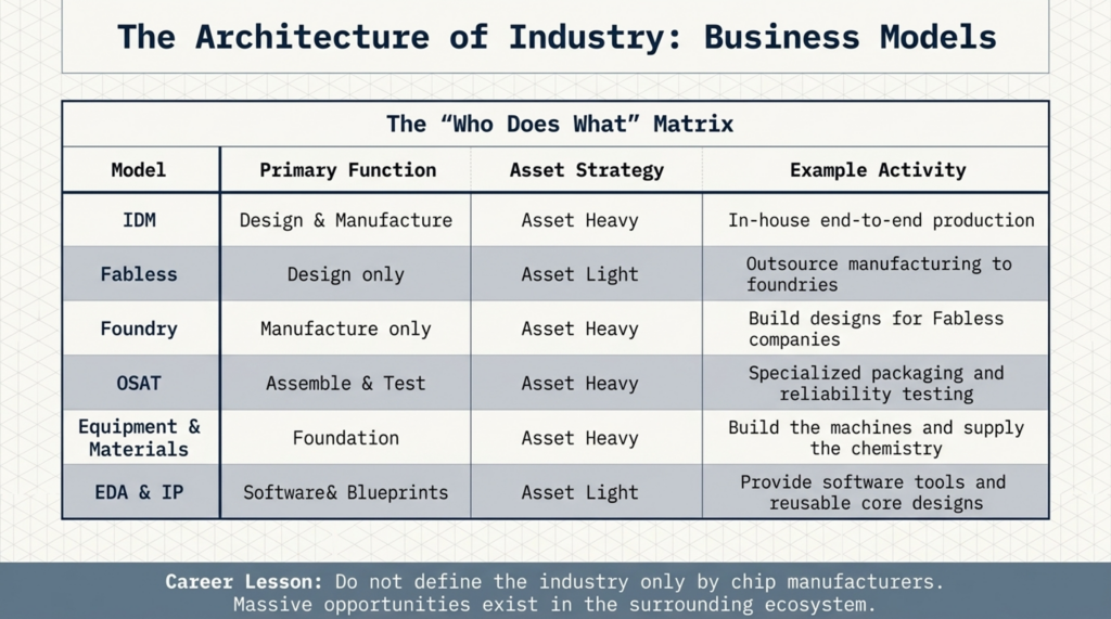
Career Lesson
Do not define the semiconductor industry only by chip manufacturers.
Some of the most important career opportunities exist in the companies surrounding the chip manufacturer.
12. The Semiconductor Industry Is Global
Semiconductors are one of the world’s most globally interconnected industries.
Design may occur in one country.
Materials may come from another.
Equipment may originate somewhere else.
Manufacturing may occur in another region.
Packaging may happen elsewhere.
The final electronic system may be assembled in yet another country.
This creates an extraordinary global network.
For future semiconductor professionals, this means understanding:
- global supply chains,
- geopolitics,
- trade,
- export controls,
- manufacturing localization,
- technology sovereignty,
- workforce development,
- international partnerships.
The semiconductor professional of the future must therefore think beyond the factory floor.
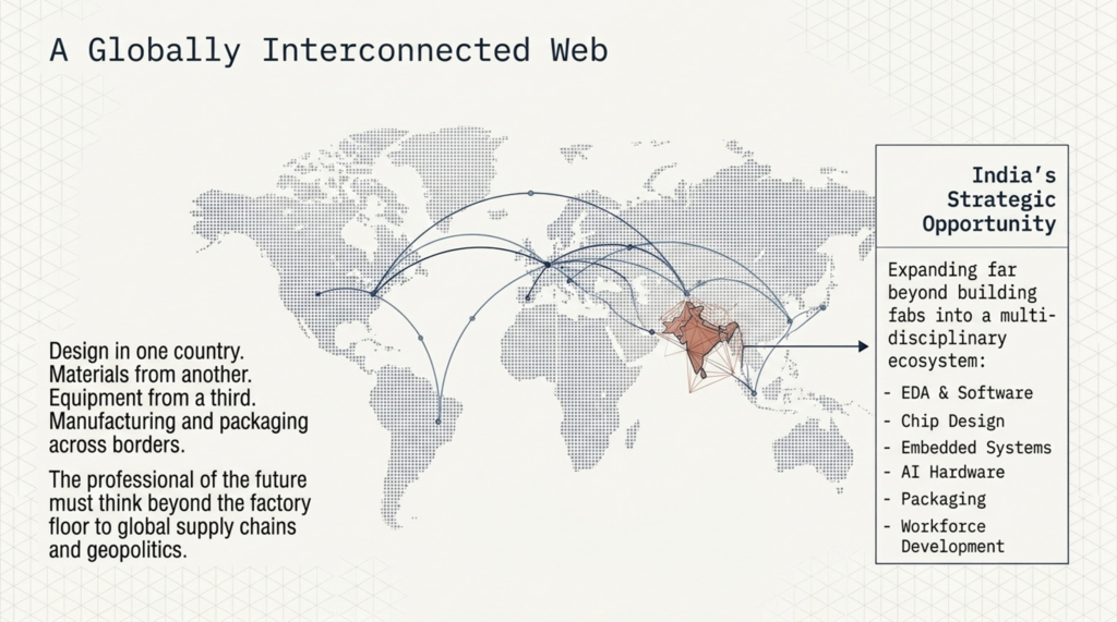
13. Why India Matters
India is entering an important phase in semiconductor development.
The opportunity is not limited to building fabs.
India can participate across the semiconductor ecosystem through:
- semiconductor design,
- EDA,
- embedded systems,
- equipment engineering,
- materials,
- wafer manufacturing,
- compound semiconductors,
- power electronics,
- semiconductor packaging,
- testing,
- automation,
- software,
- AI hardware,
- workforce development.
The opportunity is especially significant because semiconductor manufacturing requires a large multidisciplinary workforce.
This creates opportunities not only for PhDs and engineers, but also for:
- technicians,
- operators,
- software professionals,
- project managers,
- quality professionals,
- supply-chain specialists,
- sales professionals,
- finance professionals,
- educators,
- entrepreneurs.
14. The Rise of New Semiconductor Technologies
The industry is evolving rapidly.
Future semiconductor careers will increasingly be influenced by:
AI Hardware
Specialized processors and accelerators designed for AI workloads.
Silicon Carbide – SiC
Critical for power electronics, electric vehicles, renewable energy and high-efficiency power systems.
Gallium Nitride – GaN
Important for high-frequency and high-efficiency power applications.
Chiplets
Breaking complex systems into smaller interconnected semiconductor components.
Advanced Packaging
Increasing performance through innovative integration.
Heterogeneous Integration
Combining different technologies into a single system.
Edge Computing
Moving intelligence closer to sensors and devices.
Photonics
Using light for communication and computation.
Quantum Technologies
Creating new approaches to computing, sensing and communication.
Semiconductor AI
Using artificial intelligence to improve design, manufacturing, inspection and yield.
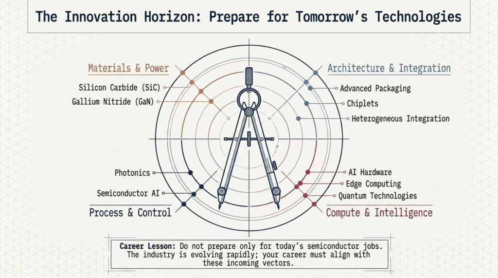
The lesson is simple:
Do not prepare only for today’s semiconductor jobs. Prepare for tomorrow’s semiconductor technologies.
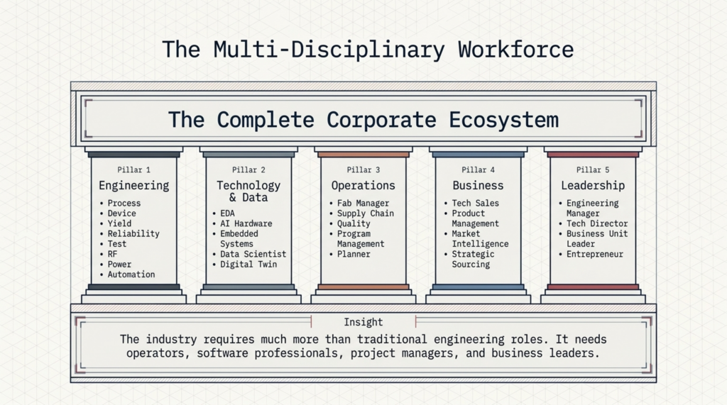
15. Where Will the Jobs Be?
The semiconductor workforce will require much more than traditional engineering roles.
Potential career paths include:
Engineering
- Semiconductor Process Engineer
- Device Engineer
- Yield Engineer
- Equipment Engineer
- Manufacturing Engineer
- Reliability Engineer
- Packaging Engineer
- Test Engineer
- Design Engineer
- Verification Engineer
- RF Engineer
- Power Electronics Engineer
- Materials Engineer
- Automation Engineer
Technology
- EDA Engineer
- AI Hardware Engineer
- Embedded Systems Engineer
- Semiconductor Software Engineer
- Data Scientist
- Digital Twin Engineer
- Manufacturing AI Specialist
Operations
- Fab Operations Manager
- Supply Chain Manager
- Quality Manager
- Program Manager
- Project Manager
- Manufacturing Planner
Business
- Semiconductor Business Development
- Technical Sales
- Product Management
- Market Intelligence
- Strategic Sourcing
- Technology Investment
- Semiconductor Consulting
Leadership
- Engineering Manager
- Manufacturing Leader
- Technology Director
- Program Director
- Business Unit Leader
- Semiconductor Entrepreneur
16. Your Career Does Not Have to Be Linear
A semiconductor career can move across the value chain.
For example:
Process Engineer → Yield Engineer → Manufacturing Manager → Fab Director
or:
Electrical Engineer → Test Engineer → Product Engineer → Product Manager
or:
Software Engineer → EDA Engineer → AI Semiconductor Engineer → Technology Leader
or:
Materials Engineer → SiC Process Engineer → Power Semiconductor Specialist → Entrepreneur
Your first job is not your final identity.
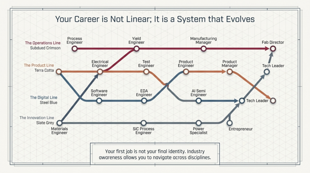
Your career is a system that evolves.
17. Build Your Semiconductor Industry Map
During Week 2, create your own Semiconductor Industry Map.
Divide a page into these sections:
- Materials
- Equipment
- Design
- EDA
- IP
- Wafer Fabrication
- Packaging
- Testing
- Systems
- Applications
- Software & AI
- Supply Chain
- Research
- Workforce & Education
Then identify companies, technologies and career opportunities in each area.
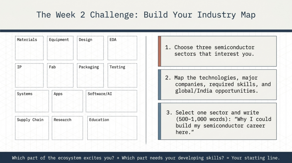
Ask yourself:
Which part of the semiconductor ecosystem excites me the most?
Then ask:
Which part of the ecosystem needs the skills I am developing?
The intersection of those two answers is where your career opportunity begins.
18. The 5 Questions Every Semiconductor Professional Should Be Able to Answer
By the end of Week 2, you should be able to answer:
Question 1
What is the semiconductor value chain?
Question 2
What are the major semiconductor technologies?
Question 3
Who are the major players and what role does each play?
Question 4
What technologies are likely to create the next generation of opportunities?
Question 5
Where do my interests and capabilities fit within this ecosystem?
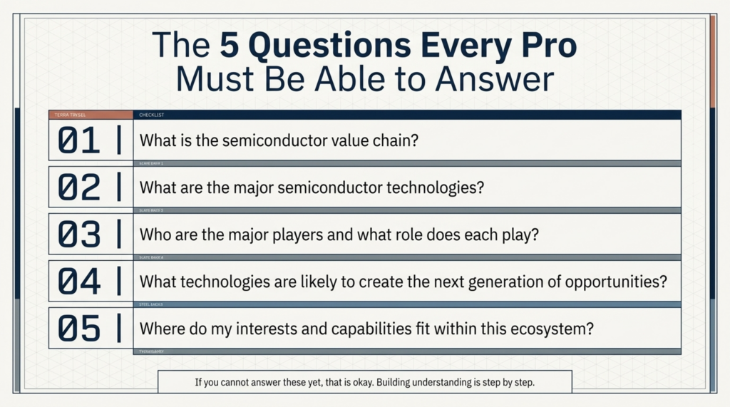
If you cannot answer these questions yet, that is okay.
That is why you are here.
NEXUS–SEMICON is about building the understanding step by step.
19. Week 2 Career Challenge
THE SEMICONDUCTOR INDUSTRY MAPPING CHALLENGE
Spend one week exploring the industry.
Your assignment:
Choose three semiconductor sectors that interest you.
For each sector, identify:
- What does this sector do?
- Why is it important?
- What technologies does it use?
- Who are the major companies?
- What skills are required?
- What jobs exist?
- What educational background is useful?
- What technologies are emerging?
- What opportunities exist in India?
- What opportunities exist globally?
Then select one sector and write:
“Why I could build my semiconductor career here.”
Keep it to 500–1,000 words.
This becomes the first serious career-positioning exercise in your NEXUS–SEMICON journey.
20. The Week 2 Mindset
Do not think:
“I need to learn everything about semiconductors.”
Think:
“I need to understand the map before choosing my route.”
You don’t need to become an expert in every technology.
You need to understand:
What exists.
How it connects.
Where it is going.
Where opportunities are emerging.
Where you can contribute.
That is industry awareness.
And industry awareness is one of the foundations of career intelligence.
21. From Week 1 to Week 2
Click here to go to Week 1 article
You discovered:
Who am I?
What am I good at?
What interests me?
What kind of impact do I want to make?
↓
WEEK 2 — KNOW THE INDUSTRY
Now we have discovered:
What is the semiconductor ecosystem?
Where are the opportunities?
What technologies are shaping the future?
Where could I fit?
COMING NEXT
UPCOMING — WEEK 3 → KNOW YOUR SKILLS
After Week 1: Know Yourself and Week 2: Know the Industry, Week 3 turns the focus toward what you can actually contribute.
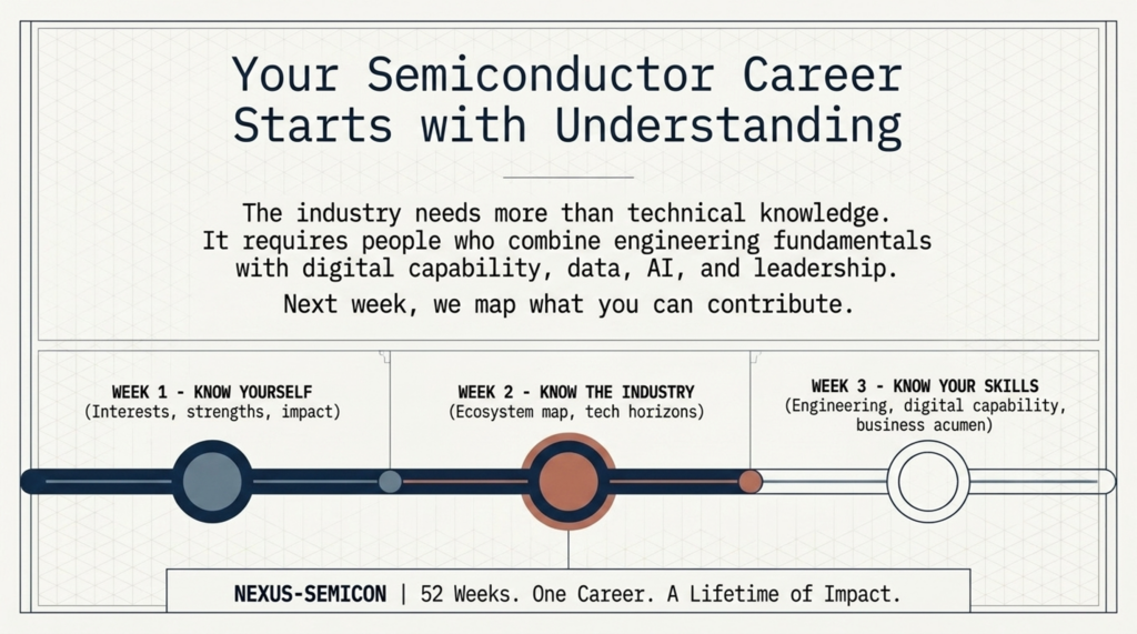
The semiconductor industry needs more than technical knowledge. It needs people who can combine engineering fundamentals, digital capabilities, software, data and AI, communication, problem-solving, project management, business understanding, and leadership.
In Week 3, you will identify the skills the industry values, assess your current capabilities, and determine what you need to develop next.
NEXUS–SEMICON
School of Next-Generation Technologies & Systems
Semiconductor Technology & Systems
52 Weeks. One Career. A Lifetime of Impact.
Your semiconductor career starts with understanding.