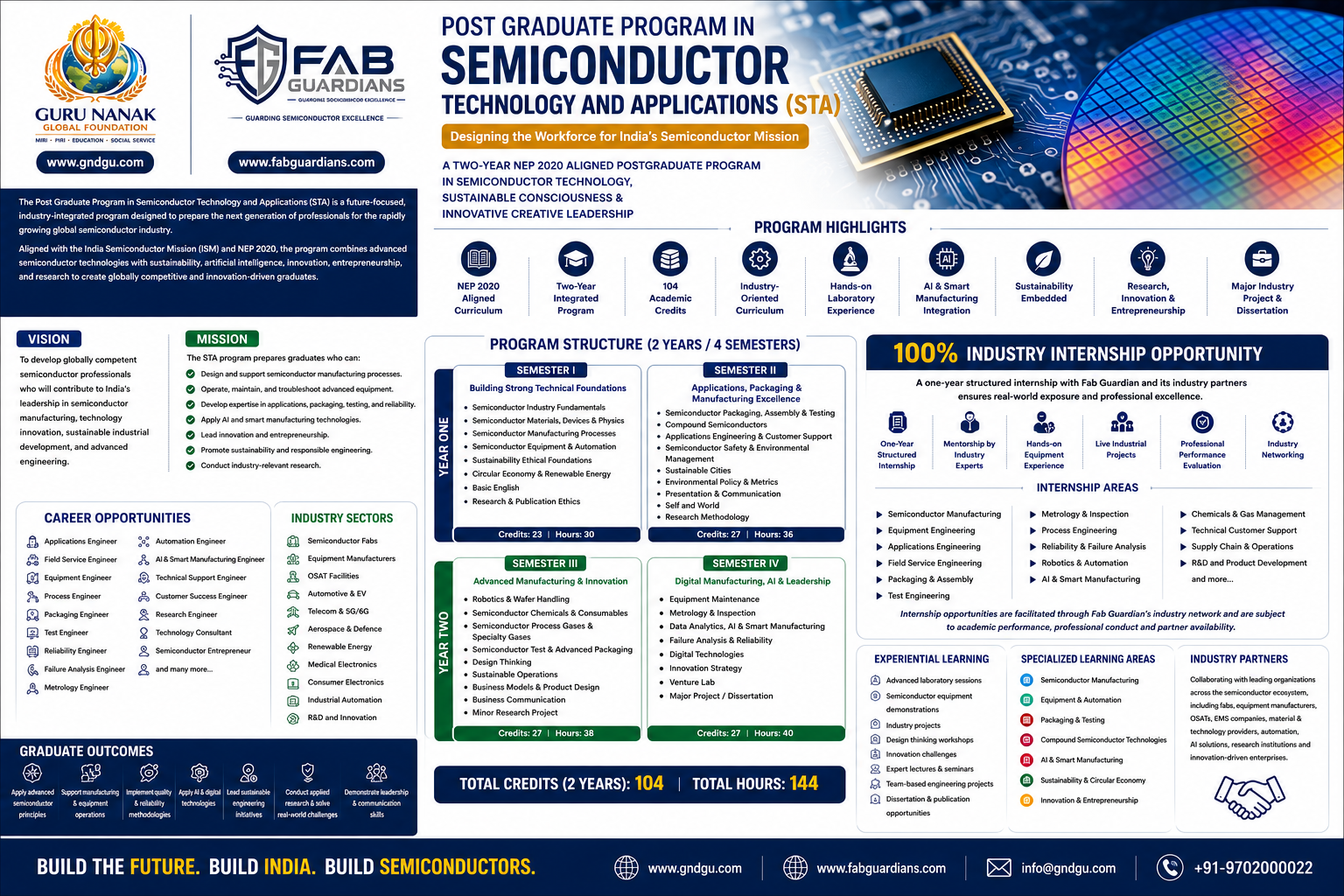
Designing the Workforce for India’s Semiconductor Mission
A Two-Year NEP 2020 Aligned Postgraduate Program in Semiconductor Technology, Sustainable Consciousness & Innovative Creative Leadership
The Post Graduate Program in Semiconductor Technology and Applications (STA) is a future-focused, industry-integrated postgraduate program designed to prepare the next generation of professionals for the rapidly growing global semiconductor industry.
Built around the vision of the India Semiconductor Mission (ISM) and aligned with the National Education Policy (NEP) 2020, the program combines advanced semiconductor technologies with sustainability, artificial intelligence, innovation, entrepreneurship, and research to create graduates who are technically proficient, globally competitive, and innovation-driven.
Students gain practical exposure to semiconductor manufacturing, equipment engineering, applications engineering, packaging, testing, automation, reliability engineering, and smart manufacturing through experiential learning, laboratory training, industry projects, and applied research.
Why Choose STA?
India is rapidly emerging as a global semiconductor hub, creating unprecedented demand for engineers and technology professionals across semiconductor manufacturing, equipment, packaging, testing, materials, automation, and AI-enabled manufacturing.
The STA program has been specifically designed to bridge the gap between academic learning and industry requirements by integrating technical expertise with leadership, sustainability, innovation, and entrepreneurial thinking.
Program Highlights
- NEP 2020 Aligned Curriculum
- Two-Year Integrated Postgraduate Program
- 104 Academic Credits
- Outcome-Based Education Framework
- Industry-Oriented Curriculum
- Hands-on Laboratory Experience
- Semiconductor Equipment Training
- AI & Smart Manufacturing Integration
- Compound Semiconductor Technologies
- Sustainability Embedded Across the Curriculum
- Research, Innovation & Entrepreneurship
- Major Industry Project & Dissertation
Program Vision
To develop globally competent semiconductor professionals who will contribute to India’s leadership in semiconductor manufacturing, technology innovation, sustainable industrial development, and advanced engineering.
Program Mission
The STA program prepares graduates who can:
- Design and support semiconductor manufacturing processes.
- Operate, maintain, and troubleshoot advanced semiconductor equipment.
- Develop expertise in semiconductor applications, packaging, testing, and reliability.
- Apply artificial intelligence and smart manufacturing technologies.
- Lead innovation and entrepreneurship within the semiconductor ecosystem.
- Promote sustainability and responsible engineering practices.
- Conduct industry-relevant research that supports technological advancement.
Program Structure
Year One
Semester I
Building Strong Technical Foundations
Students develop a comprehensive understanding of semiconductor science, manufacturing technologies, sustainability, research ethics, and communication.
Core learning areas include:
- Semiconductor Industry Fundamentals
- Semiconductor Materials, Devices & Physics
- Semiconductor Manufacturing Processes
- Semiconductor Equipment & Automation
- Sustainability Ethical Foundations
- Circular Economy & Renewable Energy
- Basic English
- Research & Publication Ethics
Semester II
Applications, Packaging & Manufacturing Excellence
Students learn advanced semiconductor applications with emphasis on packaging, safety, customer support, sustainability, and research methodology.
Key subjects include:
- Semiconductor Packaging, Assembly & Testing
- Compound Semiconductors
- Applications Engineering & Customer Support
- Semiconductor Safety & Environmental Management
- Sustainable Cities
- Environmental Policy & Metrics
- Presentation & Communication
- Self and World
- Research Methodology
Year Two
Semester III
Advanced Manufacturing & Innovation
Students develop expertise in semiconductor operations, robotics, specialty materials, process gases, advanced packaging, innovation, and research.
Subjects include:
- Robotics & Wafer Handling
- Semiconductor Chemicals & Consumables
- Semiconductor Process Gases & Specialty Gases
- Semiconductor Test & Advanced Packaging
- Design Thinking
- Sustainable Operations
- Business Models & Product Design
- Business Communication
- Minor Research Project
Semester IV
Digital Manufacturing, AI & Leadership
The final semester integrates advanced manufacturing technologies with artificial intelligence, reliability engineering, entrepreneurship, and a major research project.
Subjects include:
- Equipment Maintenance
- Metrology & Inspection
- Data Analytics, AI & Smart Manufacturing
- Failure Analysis & Reliability
- Digital Technologies
- Innovation Strategy
- Venture Lab
- Major Project / Dissertation
Experiential Learning
The STA program emphasizes practical learning through:
- Advanced laboratory sessions
- Semiconductor equipment demonstrations
- Industry projects
- Research-based learning
- Design thinking workshops
- Innovation challenges
- Case studies
- Technical seminars
- Expert lectures
- Team-based engineering projects
- Dissertation and research publication opportunities
Specialized Learning Areas
Students gain expertise across multiple domains:
Semiconductor Manufacturing
Understand wafer fabrication, manufacturing processes, contamination control, automation, quality, and production systems.
Equipment & Automation
Develop skills in semiconductor equipment, robotics, wafer handling, predictive maintenance, and factory automation.
Packaging & Testing
Learn semiconductor assembly, advanced packaging technologies, testing methodologies, and quality assurance.
Compound Semiconductor Technologies
Study GaN, SiC, GaAs, and emerging materials supporting electric vehicles, renewable energy, RF systems, aerospace, and high-performance computing.
Artificial Intelligence & Smart Manufacturing
Apply AI, machine learning, industrial analytics, and digital technologies to optimize semiconductor manufacturing operations.
Sustainability & Circular Economy
Integrate responsible manufacturing practices, environmental stewardship, renewable energy, and circular economy principles into semiconductor production.
Innovation & Entrepreneurship
Develop innovation capabilities through design thinking, product development, venture creation, and technology commercialization.
Career Opportunities
Graduates of the STA program are prepared for a wide range of careers across the semiconductor ecosystem.
Potential roles include:
- Semiconductor Applications Engineer
- Field Service Engineer
- Equipment Engineer
- Process Engineer
- Manufacturing Engineer
- Packaging Engineer
- Test Engineer
- Product Engineer
- Reliability Engineer
- Failure Analysis Engineer
- Metrology Engineer
- Automation Engineer
- Smart Manufacturing Engineer
- AI Manufacturing Engineer
- Technical Support Engineer
- Customer Success Engineer
- Research Engineer
- Technology Consultant
- Semiconductor Entrepreneur
Industry Sectors
Graduates can pursue opportunities in:
- Semiconductor Manufacturing (Fabs)
- Semiconductor Equipment Manufacturers
- Assembly, Test & Packaging (OSAT)
- Compound Semiconductor Manufacturing
- Electronics Manufacturing Services (EMS)
- Automotive Electronics
- Electric Vehicles
- Power Electronics
- Telecommunications & 5G/6G
- Aerospace & Defence
- Medical Electronics
- Renewable Energy
- Consumer Electronics
- Industrial Automation
- Research & Development
Graduate Outcomes
Upon completion of the program, graduates will be able to:
- Apply advanced semiconductor engineering principles in industrial environments.
- Support semiconductor manufacturing and equipment operations.
- Troubleshoot complex manufacturing and process challenges.
- Implement quality, reliability, and failure analysis methodologies.
- Apply AI and digital technologies in smart manufacturing.
- Lead sustainable engineering initiatives.
- Conduct applied research and solve industry challenges.
- Demonstrate leadership, communication, and entrepreneurial skills in multidisciplinary environments.
100% Industry Internship Guarantee
Learn in the Classroom. Perform in the Industry.
A distinguishing feature of the Post Graduate Program in Semiconductor Technology and Applications (STA) is its 100% industry-integrated internship pathway.
Every eligible student will undertake a structured one-year internship with Fab Guardian and its network of industry partners, providing extensive exposure to semiconductor manufacturing, equipment engineering, applications engineering, packaging, testing, reliability, automation, and smart manufacturing.
This internship is designed to bridge the gap between academic learning and real-world industrial practice, enabling students to develop the technical competencies, professional confidence, and workplace experience sought by employers.
Internship Highlights
- 100% Internship Opportunity for eligible students
- One-Year Structured Industry Internship
- Mentorship by experienced semiconductor professionals
- Exposure to advanced manufacturing facilities and semiconductor ecosystem partners
- Hands-on experience with industrial equipment, manufacturing processes, and engineering operations
- Industry-based projects aligned with academic outcomes
- Professional performance evaluation and competency development
- Opportunity to build an industry-ready portfolio
Internship Areas
Students may be placed across a range of semiconductor domains, including:
- Semiconductor Manufacturing Operations
- Semiconductor Equipment Engineering
- Applications Engineering
- Field Service Engineering
- Semiconductor Packaging & Assembly
- Test Engineering
- Metrology & Inspection
- Process Engineering
- Reliability & Failure Analysis
- Robotics & Automation
- AI & Smart Manufacturing
- Chemicals & Specialty Gas Management
- Supply Chain & Manufacturing Operations
- Technical Customer Support
- Research & Development
Industry Learning Model
The internship follows a structured progression:
Learn → Practice → Apply → Innovate → Lead
Students will:
- Work alongside experienced semiconductor engineers.
- Participate in equipment installation, maintenance, and process optimization.
- Support customer application and technical service activities.
- Contribute to quality improvement and manufacturing excellence initiatives.
- Develop technical documentation and engineering reports.
- Complete an industry-based capstone project.
Industry Partners
The internship ecosystem is coordinated by Fab Guardian in collaboration with its semiconductor ecosystem partners, including organizations involved in:
- Semiconductor Manufacturing
- Semiconductor Equipment
- Assembly, Test & Packaging (OSAT)
- Compound Semiconductor Technologies
- Electronics Manufacturing Services (EMS)
- Semiconductor Materials & Consumables
- Cleanroom & Facility Engineering
- Automation & Smart Manufacturing
- Industrial AI Solutions
- Semiconductor Research & Development
Internship placements are facilitated through Fab Guardian’s industry network and are subject to academic performance, professional conduct, organizational requirements, and partner availability.
Career Advantage
Upon completion of the program and internship, graduates will possess:
- Up to one year of structured industry experience
- Hands-on exposure to semiconductor manufacturing environments
- Practical engineering and troubleshooting skills
- Professional workplace competencies
- Industry mentoring and networking opportunities
- A strong foundation for careers in semiconductor manufacturing, equipment, applications, quality, and advanced engineering
From Classroom to Cleanroom
Through Fab Guardian and its industry partners, the STA program combines academic excellence with immersive industrial experience—preparing graduates to contribute from day one to India’s rapidly growing semiconductor ecosystem.
Program at a Glance
| Feature | Details |
|---|---|
| Program | Post Graduate Program in Semiconductor Technology and Applications (STA) |
| Duration | 2 Years (4 Semesters) |
| Academic Credits | 104 |
| Framework | NEP 2020 Aligned |
| Learning Model | Outcome-Based, Multidisciplinary & Experiential |
| Research | Research Methodology, Proposal & Dissertation |
| Core Themes | Semiconductor Technology, Sustainability, AI, Innovation & Leadership |
Join the Future of Semiconductor Innovation
The semiconductor industry is transforming the world—from smartphones and electric vehicles to artificial intelligence, renewable energy, medical devices, aerospace, and advanced computing. The Post Graduate Program in Semiconductor Technology and Applications (STA) equips graduates with the knowledge, technical expertise, research capability, and leadership mindset needed to thrive in this rapidly evolving landscape.
Be part of India’s semiconductor revolution. Build technologies that shape the future.